BUK9506-55B
BUK9506-55B is (BUK9x06-55B) N-channel TrenchMOSTM logic level FET manufactured by NXP Semiconductors.
description
N-channel enhancement mode field-effect power transistor in a plastic package using Philips High-Performance Automotive (HPA) Trench MOS™ technology, featuring very low on-state resistance.
1.2 Features s Trench MOS™ technology s 175 °C rated s Q101 pliant s Logic level patible.
1.3 Applications s Automotive systems s Motors, lamps and solenoids s 12 V and 24 V loads s General purpose power switching.
1.4 Quick reference data s EDS(AL)S ≤ 679 m J s ID ≤ 75 A s RDSon = 5.1 mΩ (typ) s Ptot ≤ 258 W.
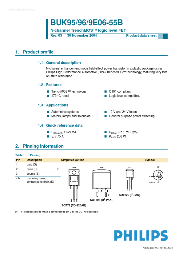
2. Pinning information
Table 1: Pin 1 2 3 mb Pinning Description gate (G) drain (D) source (S) mounting base; connected to drain (D)
[1]
Simplified outline mb mb
Symbol mb
G mbb076
2 1 1 2 3
SOT226 (I2-PAK)
SOT404 (D2-PAK)
SOT78 (TO-220AB)
[1] It is not possible to make a connection to pin 2 of the SOT404 package.
..
Philips Semiconductors
BUK95/96/9E06-55B
N-channel Trench MOS™ logic level FET
3. Ordering information
Table 2: Ordering information Package Name BUK9506-55B BUK9606-55B BUK9E06-55B TO-220AB D2-PAK I2-PAK Description
Plastic single-ended package; heatsink mounted; 1 mounting hole; 3-lead TO-220AB Version SOT78 Type number
Plastic single-ended surface mounted package (Philips version of D2-PAK); SOT404 3 leads (one lead cropped) Plastic single-ended package (Philips version of I2-PAK); low-profile 3 lead TO-220AB SOT226
4. Limiting values
Table 3: Limiting values In accordance with the Absolute Maximum Rating System (IEC 60134). Symbol Parameter VDS VDGR VGS ID drain-source voltage (DC) drain-gate voltage (DC) gate-source voltage (DC) drain current (DC) Tmb = 25 °C; VGS = 5 V; Figure 2 and 3 Tmb = 100 °C; VGS = 5 V; Figure 2 IDM Ptot Tstg Tj IDR IDRM peak drain current total power dissipation storage temperature junction temperature reverse drain current (DC) peak reverse drain current Tmb = 25 °C Tmb = 25 °C; pulsed; tp ≤ 10 µs unclamped inductive load; ID = 75 A; VDS ≤ 55 V; RGS = 50 Ω; VGS = 5 V; starting at Tj = 25 °C
[1]...