BUK9880-55A
BUK9880-55A is TrenchMOS logic level FET manufactured by NXP Semiconductors.
Description
N-channel enhancement mode field-effect power transistor in a plastic package using Trench MOS™1 technology, featuring very low on-state resistance. Product availability: BUK9880-55A in SOT223 (SC-73).
2. Features s s s s Trench MOS™ technology Q101 pliant 150 °C rated Logic level patible.
3. Applications s Automotive and general purpose power switching: x 12 V and 24 V loads x Motors, lamps and solenoids. c c
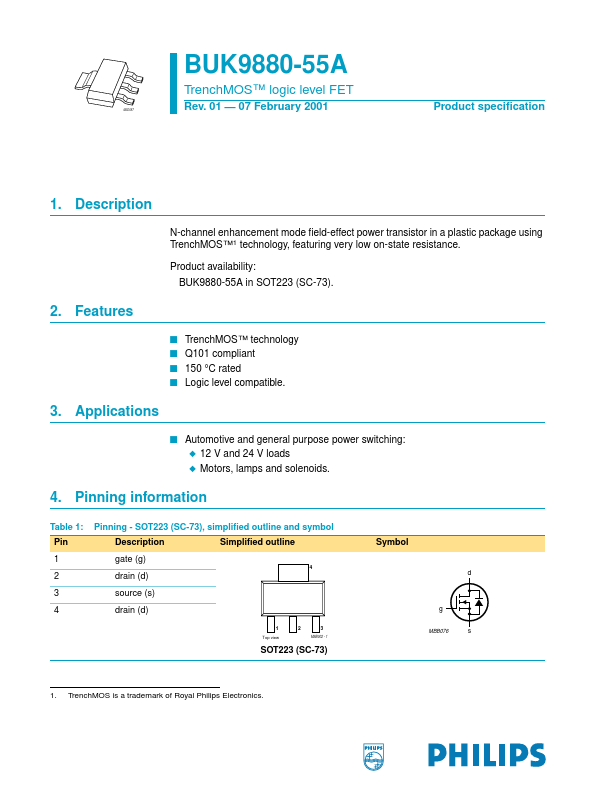
4. Pinning information
Table 1: Pin 1 2 3 4 Pinning
- SOT223 (SC-73), simplified outline and symbol Description gate (g)
Simplified outline
Symbol drain (d) source (s) drain (d)
Top view d g
2 3
MSB002
- 1
MBB076 s
SOT223 (SC-73)
1.
Trench MOS is a trademark of Royal Philips Electronics.
Philips Semiconductors
Trench MOS™ logic level FET
5. Quick reference data
Table 2: VDS ID Ptot Tj RDSon Quick reference data Conditions Tsp = 25 °C; VGS = 5 V Tsp = 25 °C VGS = 5 V; ID = 8 A; Tj = 25 °C VGS = 4.5 V; ID = 8 A; Tj = 25 °C VGS = 10 V; ID = 8 A; Tj = 25 °C Typ
- -
- - 68
- - Max 55 7 8 150 80 89 73 Unit V A W °C drain-source voltage (DC) drain current (DC) total power dissipation junction temperature drain-source on-state resistance Symbol Parameter mΩ mΩ mΩ
6. Limiting values
Table 3: Limiting values In accordance with the Absolute Maximum Rating System (IEC 60134). Symbol Parameter VDS VDGR VGS VGSM ID IDM Ptot Tstg Tj IDR IDRM WDSS drain-source voltage (DC) drain-gate voltage (DC) gate-source voltage (DC) non-repetitive gate-source voltage drain current (DC) peak drain current total power dissipation storage temperature operating junction temperature reverse drain current (DC) pulsed reverse drain current non-repetitive avalanche energy Tsp = 25 °C Tsp = 25 °C; pulsed; tp ≤ 10 µs unclamped inductive load; ID = 6 A; VDS ≤ 55 V; VGS = 5 V; RGS = 50 Ω; starting Tsp = 25 °C tp ≤ 50 µs Tsp = 25 °C; VGS = 5 V;Figure 2 and 3 Tsp = 100 °C; VGS = 5 V; Figure 2 Tsp = 25 °C; pulsed tp ≤ 10 µs; Figure 3 Tsp = 25 °C; Figure 1 RGS =...