NXP Semiconductors CBT3306
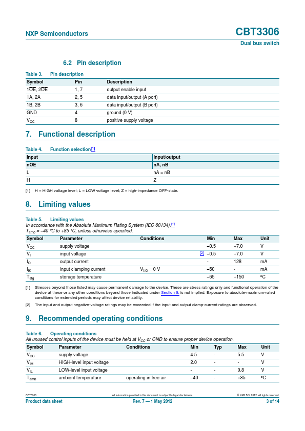
The CBT3306 dual FET bus switch features independent line switches. Each switch is disabled when the associated output enable (nOE) input is HIGH. The CBT3306 is characterized for operation from 40 C to +85 C.| Part No. | CBT3306 |
|---|---|
| Datasheet | CBT3306 Download |
| Manufacturer |  NXP Semiconductors |
| Description | Dual bus switch |
| Buy | Stock & Price |
FEATURES AND BENEFITS
● 5 switch connection between two ports● TTL-compatible input levels
● Multiple package options
● Latch-up protection exceeds 100 mA per JESD78B
● ESD protection:
● HBM JESD22-A114F exceeds 2000 V
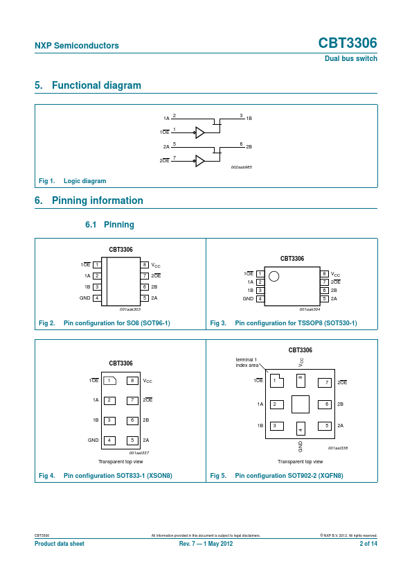
● CDM JESD22-C101D exceeds 1000 V 3. Ordering information Table 1. Ordering information Type number Package Name CBT3306D SO8 CBT3306PW TSSOP8 CBT3306GT XSON8 CBT3306GM XQFN8
DESCRIPTION
plastic small outline package; 8 leads; body width 3.9 mm plastic thin shrink small outline package; 8 leads; body width 4.4 mm plastic extremely thin small outline package; no leads; 8 terminals; body 1 1.95 0.5 mm plastic, extremely thin quad flat package; no leads; 8 terminals; body 1.6 1.6 0.5 mm Version SOT96-1 SOT530-1 SOT833-1 SOT902-2 4. Marking Table 2. Marking codes Type number CBT3306D CBT3306PW CBT3306GT CBT3306GM Marking code CBT3306 3306 F06 F06 NXP Semiconductors 5. Functional diagram 1A 2 1OE 1 2A 5 2OE 7 Fig 1. Logic diagram 6. Pinning information 6.1 Pinning CBT3306 1OE 1 1A 2 1B 3 GND 4 8 VCC 7 2OE 6 2B 5 2A 001aak303 Fig 2.