NXP Semiconductors CBTD3306
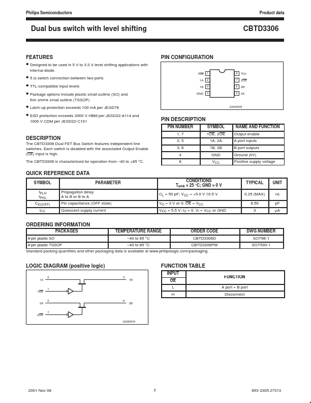
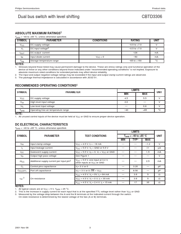
The CBTD3306 Dual FET Bus Switch features independent line switches. Each switch is disabled with the associated Output Enable (OE) input is high. The CBTD3306 is characterized for operation from –40 to +85 °C.| Part No. | CBTD3306 |
|---|---|
| Datasheet | CBTD3306 Download |
| Manufacturer |  NXP Semiconductors |
| Description | Dual bus switch |
| Buy | Stock & Price |
FEATURES
● Designed to be used in 5 V to 3.3 V level shifting applications with internal diode. PIN CONFIGURATION 1OE 1A 1B GND 1 2 3 4 8 7 6 5 VCC 2OE 2B 2A● 5 Ω switch connection between two ports
● TTL-compatible input levels
● Package options include plastic small outline (SO) and thin shrink small outline (TSSOP)
● Latch-up protection exceeds 100 mA per JESD78
● ESD protection exceeds 2000 V HBM per JESD22-A114 and 1000 V CDM per JESD22-C101 SA00535 PIN
DESCRIPTION
PIN NUMBER SYMBOL 1OE, 2OE 1A, 2A 1B, 2B GND VCC NAME AND FUNCTION Output enable A port inputs B port outputs Ground (0V) Positive supply voltage 1, 7 2, 5 3, 6 4 8DESCRIPTION
QUICK REFERENCE DATA SYMBOL tPLH tPHL CIO(OFF) ICC Propagation delay A to B or B to A Pin capacitance (OFF state) Quiescent supply current PARAMETER CONDITIONS Tamb = 25 °C; GND = 0 V CL = 50 pF; VCC = +5.0 V ±0.5 V VO = 3 V or 0; OE = VCC VCC = 5.5 V; IO = 0, VI = VCC or GND TYPICAL 0.25 (MAX) 6.50 3 UNIT ns pF µA ORDERING INFORMATION PACKAGES...