NXP Semiconductors CBTV4010
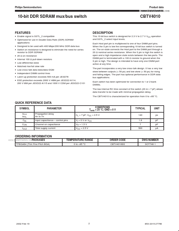
The CBTV4010 is characterized for operation from 0 to +85 °C. These are stress ratings only and functional operation of the device at these or any other conditions beyond those indicated under “recommended operating conditions” is not implied.| Part No. | CBTV4010 |
|---|---|
| Datasheet | CBTV4010 Download |
| Manufacturer |  NXP Semiconductors |
| Description | 10-bit DDR SDRAM mux/bus switch |
| Buy | Stock & Price |
FEATURES
● Enable signal is SSTL_2 compatible● Optimized for use in Double Data Rate (DDR) SDRAM applications
● Designed to be used with 400 Mbps/200 MHz DDR data bus
● Switch on resistance is designed to eliminate the need for series resistor to DDR SDRAM
● 20 Ω on resistance
● Internal 100 Ω pull-down resistors
● Low differential skew
● Matched rise/fall slew rate
● Low cross-talk data-data/data-DQM
● Independent DIMM control lines
● Latch-up protection exceeds 500 mA per JESD78
● ESD protection exceeds 2000 V HBM per JESD22-A114, 200 V MM per JESD22-A115 and 1000 V CDM per JESD22-C101
DESCRIPTION
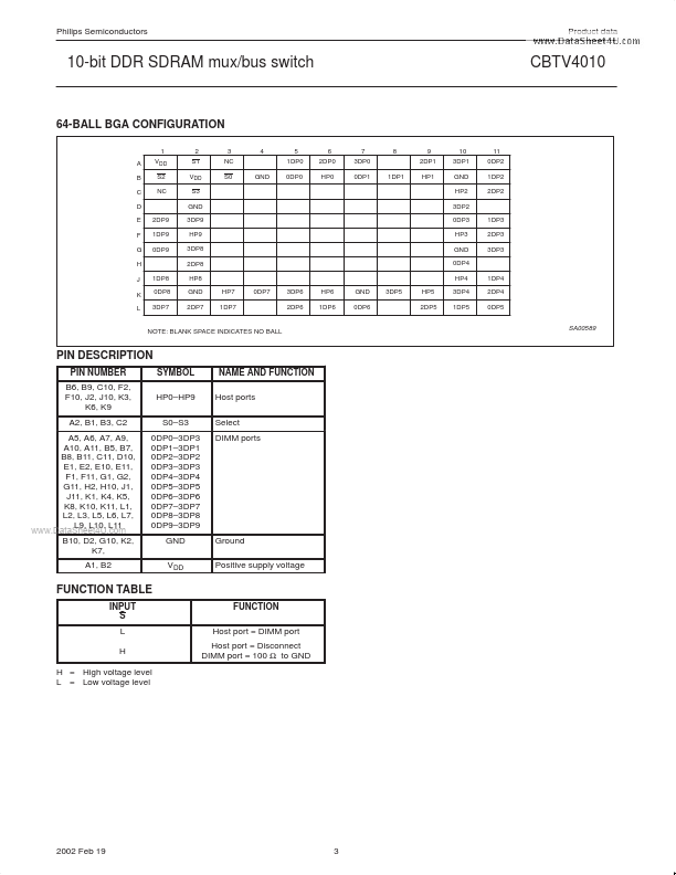
This 10-bit bus switch is designed for 2.3 V to 2.7 V VCC operation and SSTL_2 select input levels. Each Host port pin is multiplexed to one of four DIMM port pins. When the S pin is low the corresponding 10-bit bus switch is turned on. The on-state connects the Host port to the DIMM port through a 20 Ω nominal series resistance. When the S pin is high the switch is open and a high-impedance state exists between the two ports.