NXP Semiconductors DAC1627D1G25
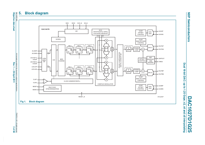
The DAC1627D1G25 is a high-speed 16-bit dual channel Digital-to-Analog Converter (DAC) with selectable ×2, ×4 and ×8 interpolating filters optimized for multi-carrier and broadband wireless transmitters at sample rates of up to 1.25 Gsps. The DAC1627D1G25 is capable of meeting multi-carrier GSM specifications. For example, with an output frequency of 150 MHz and a DAC clock frequency of 1.22 Gsps the full-scale dynamic range is: • SFDRRBW = 85 dBc (bandwidth = 250 MHz) • IMD3 = 85 dBc The Serial Peripheral Interface (SPI) provides full control of the DAC1627D1G25.| Part No. | DAC1627D1G25 |
|---|---|
| Datasheet | DAC1627D1G25 Download |
| Manufacturer |  NXP Semiconductors |
| Description | Dual 16-bit DAC |
| Buy | Stock & Price |
FEATURES AND BENEFITS
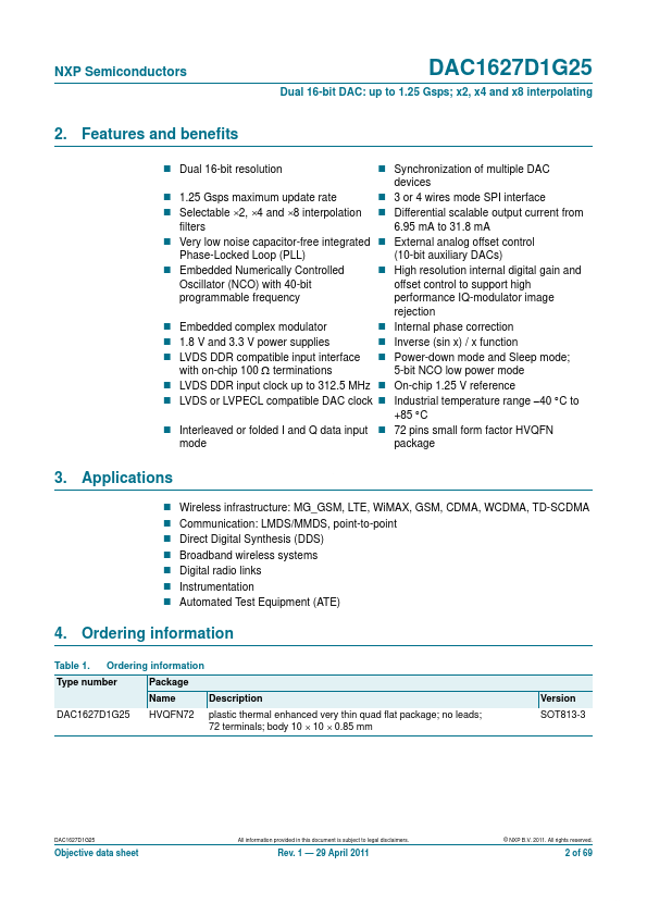
Dual 16-bit resolution 1.25 Gsps maximum update rate Selectable ×2, ×4 and ×8 interpolation filters Very low noise capacitor-free integrated Phase-Locked Loop (PLL) Embedded Numerically Controlled Oscillator (NCO) with 40-bit programmable frequency Embedded complex modulator 1.8 V and 3.3 V power supplies LVDS DDR compatible input interface with on-chip 100 Ω terminations LVDS DDR input clock up to 312.5 MHz LVDS or LVPECL compatible DAC clock Interleaved or folded I and Q data input mode Synchronization of multiple DAC devices 3 or 4 wires mode SPI interface Differential scalable output current from 6.95 mA to 31.8 mA External analog offset control (10-bit auxiliary DACs) High resolution internal digital gain and offset control to support high performance IQ-modulator image rejection Internal phase correction Inverse (sin x) / x function Power-down mode and Sleep mode; 5-bit NCO low power mode On-chip 1.25 V reference Industrial temperature range −40 °C to +85 °C 72 pins small form factor HVQFN package 3.