NXP Semiconductors DC6M501X6
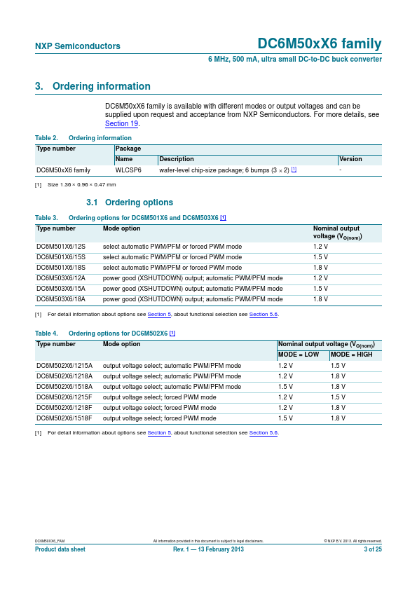
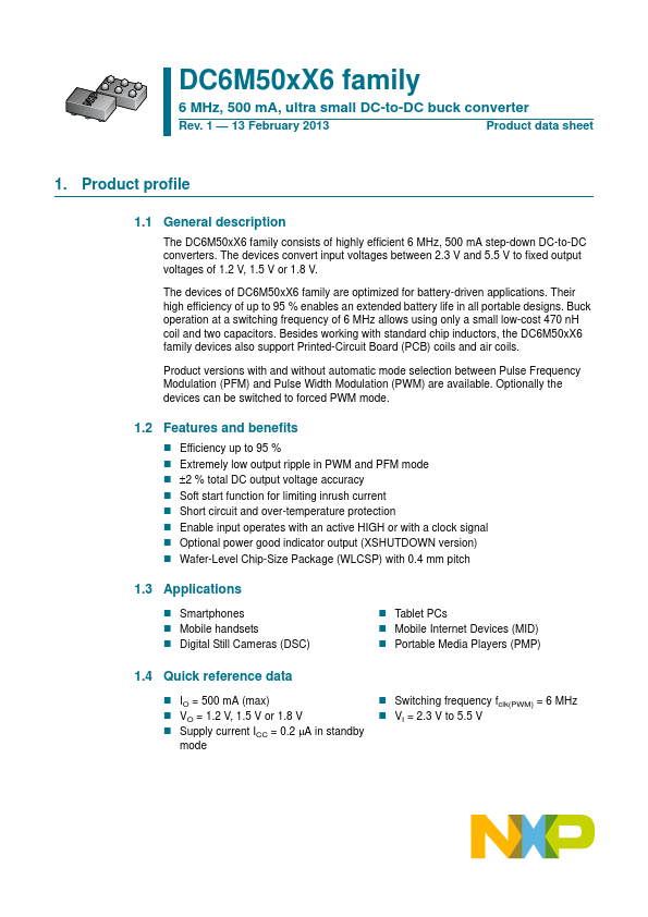
The DC6M50xX6 family consists of highly efficient 6 MHz, 500 mA step-down DC-to-DC converters. The devices convert input voltages between 2.3 V and 5.5 V to fixed output voltages of 1.2 V, 1.5 V or 1.8 V. The devices of DC6M50xX6 family are optimized for battery-driven applications.| Part No. | DC6M501X6 |
|---|---|
| Datasheet | DC6M501X6 Download |
| Manufacturer |  NXP Semiconductors |
| Description | ultra small DC-to-DC buck converter |
| Buy | Stock & Price |
FEATURES AND BENEFITS
● Efficiency up to 95 %● Extremely low output ripple in PWM and PFM mode
● 2 % total DC output voltage accuracy
● Soft start function for limiting inrush current
● Short circuit and over-temperature protection
● Enable input operates with an active HIGH or with a clock signal
● Optional power good indicator output (XSHUTDOWN version)
● Wafer-Level Chip-Size Package (WLCSP) with 0.4 mm pitch 1.3
APPLICATIONS
● Smartphones● Mobile handsets
● Digital Still Cameras (DSC)
● Tablet PCs
● Mobile Internet Devices (MID)
● Portable Media Players (PMP) 1.4 Quick reference data
● IO = 500 mA (max)
● VO = 1.2 V, 1.5 V or 1.8 V
● Supply current ICC = 0.2 A in standby mode
● Switching frequency fclk(PWM) = 6 MHz
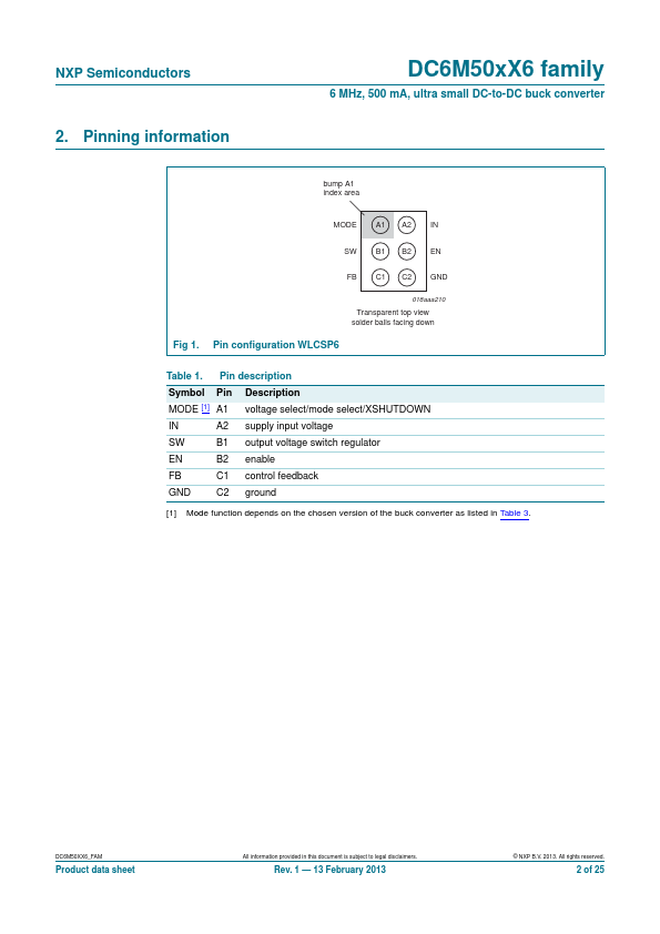
● VI = 2.3 V to 5.5 V NXP Semiconductors 2. Pinning information DC6M50xX6 family 6 MHz, 500 mA, ultra small DC-to-DC buck converter bump A1 index area MODE A1 A2 IN SW B1 B2 EN FB C1 C2 GND 018aaa210 Transparent top view solder balls facing down Fig 1. Pin configuration WLCSP6 Table 1.