NXP Semiconductors FBL2033
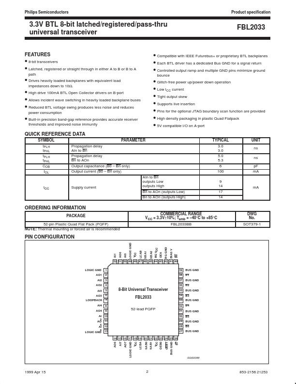
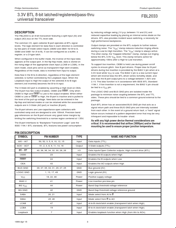
The FBL2033 is an 8-bit transceiver featuring a split input (AI) and output (AO) bus on the TTL-level side. The common I/O, open collector B port operates at BTL signal levels. The logic element for data flow in each direction is controlled by two pairs of mode select inputs (SBA0 and SBA1 for B-to-A, SAB0 and SAB1 for A-to-B).| Part No. | FBL2033 |
|---|---|
| Datasheet | FBL2033 Download |
| Manufacturer |  NXP Semiconductors |
| Description | 3.3V BTL 8-bit latched/registered/pass-thru universal transceiver |
| Buy | Stock & Price |
FEATURES
● 8-bit transceivers● Latched, registered or straight through in either A to B or B to A path
● Compatible with IEEE Futurebus+ or proprietary BTL backplanes
● Each BTL driver has a dedicated Bus GND for a signal return
● Controlled output ramp and multiple GND pins minimize ground bounce
● Drives heavily loaded backplanes with equivalent load
● High drive 100mA BTL Open Collector drivers on B-port
● Allows incident wave switching in heavily loaded backplane buses
● Reduced BTL voltage swing produces less noise and reduces power consumption impedances down to 10Ω.
● Built-in precision band-gap reference provides accurate receiver thresholds and improved noise immunity
● Glitch-free power up/power down operation
● Low ICC current
● Tight output skew
● Supports live insertion
● Pins for the optional JTAG boundary scan function are provided
● High density packaging in plastic Quad Flatpack
● 5V compatible I/O on A-port TYPICAL 3.0 3.0 5.0 5.3 6 100 9 14 17 14 UNIT ns ns pF mA QU...