FEATURES
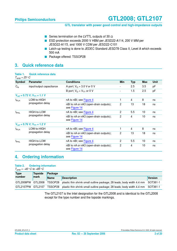
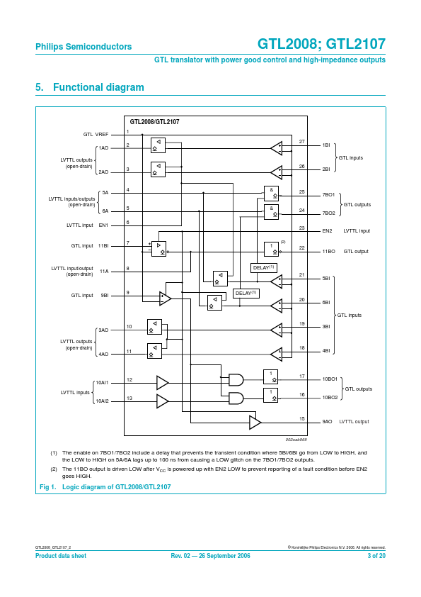
I Operates as a GTL to LVTTL sampling receiver or LVTTL to GTL driver I EN1 and EN2 disable error output I All LVTTL and GTL outputs are put in a high-impedance state when EN1 and EN2 are LOW I 3.0 V to 3.6 V operation I LVTTL I/O not 5 V tolerant DataSheet 4 U .com Philips Semiconductors GTL2008; GTL2107 GTL translator with power good control and high-impedance outputs I Series termination on the LVTTL outputs of 30 Ω I ESD protection exceeds 2000 V HBM per JESD22-A114, 200 V MM per JESD22-A115, and 1000 V CDM per JESD22-C101 I Latch-up testing is done to JEDEC Standard JESD78 Class II, Level A which exceeds 500 mA I Package offered: TSSOP28 3. Quick reference data Table 1. Quick reference data Tamb = 25 °C Symbol Cio Parameter input/output capacitance Conditions A port; VO = 3.0 V or 0 V B port; VO = VTT or 0 V Vref = 0.73 V; VTT = 1.1 V tPLH LOW-to-HIGH propagation delay HIGH-to-LOW propagation delay nA to nBI; see Figure 4 nBI to nA or nAO (open-drain outputs); see Figure... NXP Semiconductors