DESCRIPTION
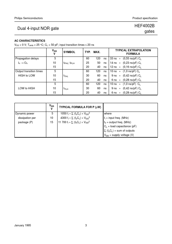
HEF4002B gates Fig.2 Pinning diagram. HEF4002BP(N): HEF4002BD(F): HEF4002BT(D): Fig.1 Functional diagram. 14-lead DIL; plastic (SOT27-1) 14-lead DIL; ceramic (cerdip) (SOT73) 14-lead SO; plastic (SOT108-1) ( ): Package Designator North America Fig.3 Logic diagram (one gate). FAMILY DATA, IDD LIMITS category GATES See Family Specifications January 1995 2 Philips Semiconductors Product specification Dual 4-input NOR gate AC CHARACTERISTICS VSS = 0 V; Tamb = 25 °C; CL = 50 pF; input transition times ≤ 20 ns VDD V Propagation delays In → On Output transition times HIGH to LOW 5 10 15 5 10 15 5 LOW to HIGH 10 15 tTLH tTHL tPHL; tPLH SYMBOL TYP. 60 25 20 60 30 20 60 30 20 MAX. 120 50 40 120 60 40 120 60 40 ns ns ns ns ns ns ns ns ns HEF4002B gates TYPICAL EXTRAPOLATION FORMULA 33 ns + (0,55 ns/pF) CL 14 ns + (0,23 ns/pF) CL 12 ns + (0,16 ns/pF) CL 10 ns + (1,0 ns/pF) CL 9 ns + (0,42 ns/pF) CL 6 ns + (0,28 ns/pF) CL 10 ns + (1,0 ns/pF) CL 9 ns + (0,42 ns/pF) CL 6 ns + (0,28 ns/pF) C... NXP Semiconductors