DESCRIPTION
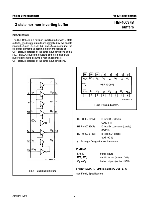
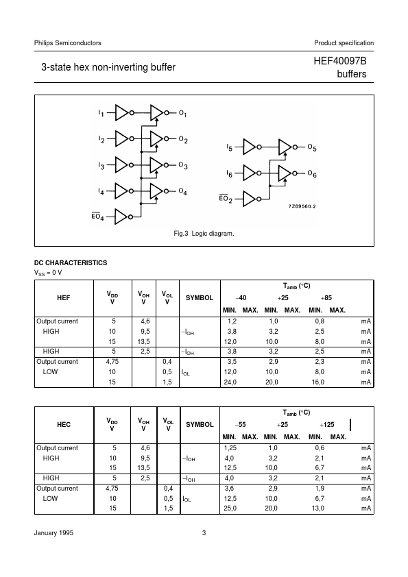
A HIGH on EO4 causes four of the six buffer elements to assume a high impedance or OFF-state, regardless of the other input conditions and a HIGH on EO2 causes the outputs of the remaining two buffer elements to assume a high impedance or OFF-state, regardless of the other input conditions. HEF40097B buffers Fig.2 Pinning diagram. HEF40097BP(N): HEF40097BD(F): HEF40097BT(D): 16-lead DIL; plastic (SOT38-1) 16-lead DIL; ceramic (cerdip) (SOT74) 16-lead SO; plastic (SOT109-1) ( ): Package Designator North America PINNING I1 to I6 EO4, EO2 O1 to O6 buffer inputs enable inputs (active LOW) buffer outputs (active HIGH) Fig.1 Functional diagram. FAMILY DATA, IDD LIMITS category BUFFERS See Family Specifications January 1995 2 Philips Semiconductors Product specification 3-state hex non-inverting buffer HEF40097B buffers Fig.3 Logic diagram. DC CHARACTERISTICS VSS = 0 V Tamb (°C) HEF VDD V 5 10 15 HIGH Output current LOW 5 4,75 10 15 VOH V 4,6 9,5 13,5 2,5 0,4 0,5 1,5 IOL −IOH −IOH VOL V SYMBOL −40 +25 +85 MIN. NXP Semiconductors