DESCRIPTION
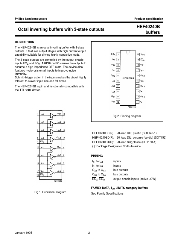
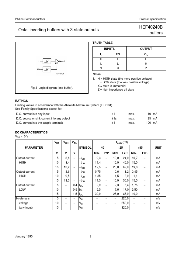
A HIGH on EO causes the outputs to assume a high impedance OFF-state. The device also features hysteresis on all inputs to improve noise immunity. Schmitt-trigger action in the inputs makes the circuit highly tolerant to slower input rise and fall times. The HEF40240B is pin and functionally compatible with the TTL ‘240’ device. HEF40240B buffers Fig.2 Pinning diagram. HEF40240BP(N): 20-lead DIL; plastic (SOT146-1) HEF40240BD(F): 20-lead DIL; ceramic (cerdip) (SOT152) HEF40240BT(D): 20-lead SO; plastic (SOT163-1) ( ): Package Designator North America PINNING IA1 to IA4 IB1 to IB4 OA1 to OA4 OB1 to OB4 EOA, EOB inputs inputs bus outputs bus outputs output enable inputs (active LOW) FAMILY DATA, IDD LIMITS category buffers Fig.1 Functional diagram. See Family Specifications January 1995 2 Philips Semiconductors Product specification Octal inverting buffers with 3-state outputs TRUTH TABLE INPUTS In H L X Notes EO L L H HEF40240B buffers OUTPUT On L H Z Fig.3 Logic diagram (one buffer). NXP Semiconductors