NXP Semiconductors J211
This product is supplied in anti-static packing to prevent damage caused by electrostatic discharge during transport and handling. For further information, refer to Philips specs.: SNW-EQ-608, SNW-FQ-302A and SNW-FQ-302B.| Part No. | J211 |
|---|---|
| Datasheet | J211 Download |
| Manufacturer |  NXP Semiconductors |
| Description | N-channel field-effect transistors |
| Buy | Stock & Price |
FEATURES
● High speed switching● Interchangeability of drain and source connections
● High impedance.
APPLICATIONS
● Analog switches● Choppers, multiplexers and commutators
● Audio amplifiers.
DESCRIPTION
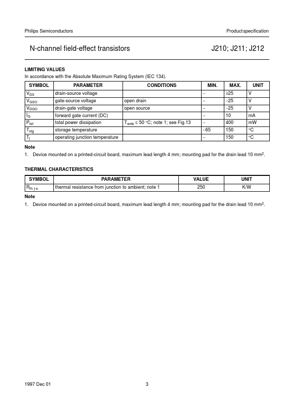
N-channel symmetrical junction field-effect transistor in a TO-92 (SOT54) package. CAUTION Marking codes: J210: J210. J211: J211. J212: J212. handbook, halfpage 2 J210; J211; J212 PINNING - TO-92 (SOT54) PIN 1 2 3 SYMBOL g s d gate source drainDESCRIPTION
1 3 g MAM197 d s Fig.1 Simplified outline and symbol. QUICK REFERENCE DATA SYMBOL VDS VGSoff PARAMETER drain-source voltage gate-source cut-off voltage J210 J211 J212 IDSS drain current J210 J211 J212 Ptot yfs total power dissipation common-source transfer admittance J210 J211 J212 Tamb ≤ 50 °C VGS = 0; VDS = 15 V 4 6 7 12 12 12 mS mS mS VGS = 0; VDS = 15 V 2 7 15 − 15 20 40 400 mA mA mA mW ID = 1 nA; VDS = 15 V −1 −2.5 −4 −3 −4.5 −6 V V V CONDITIONS − MIN. MAX. ±25 UNIT V 1997 Dec 01 2 Philips Semiconductors Product specification N-channel field-effect transistors LIMITING VALUES In accordance with the Absolute Maximum Rating System (IEC 134).