NXP Semiconductors MC32BC3770
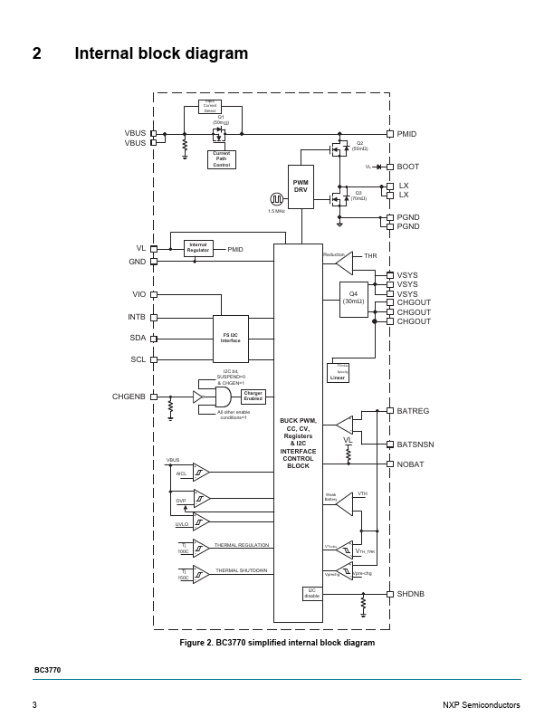
The two VBUS pins must be connected together externally. These pins are used as an output in OTG mode.| Part No. | MC32BC3770 |
|---|---|
| Datasheet | MC32BC3770 Download |
| Manufacturer |  NXP Semiconductors |
| Description | 2.0A switch-mode charger |
| Buy | Stock & Price |
FEATURES
● Dual-path output to power-up system in dead battery● Single input for USB/TA
● High-efficiency synchronous switching regulator
● 20 V maximum withstanding input voltage
● Minimize the charging time with remote sense
● Up to 2.0 A load current for system or battery
● Programmable charge parameters via I2C compatible interface
● 400 kHz full-speed I2C interface
● 1.5 MHz switching frequency
● Charge reduction mode for maximizing charging efficiency BATTERY CHARGER CS SUFFIX 98ASA00848D 25 WLCSP
APPLICATIONS
● Internet of things (IoT)● Handheld consumer devices
● Wearable application
● mPOS terminals
● Medical portable equipment
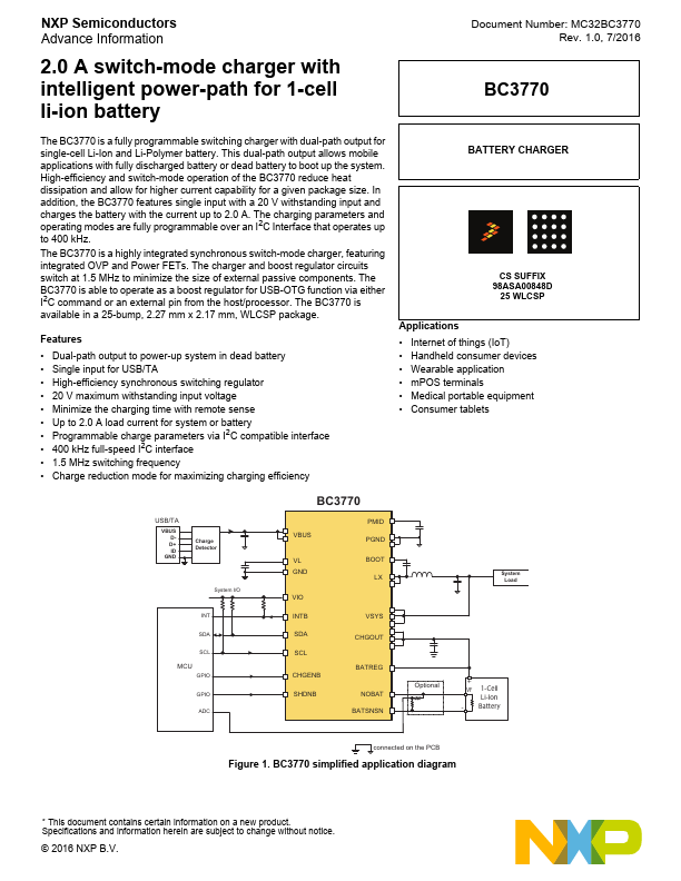
● Consumer tablets USB/TA VBUS DD+ ID GND Charge Detector System I/O INT SDA SCL MCU GPIO GPIO ADC BC3770 VBUS PMID PGND VL GND BOOT LX VIO INTB SDA SCL CHGENB VSYS CHGOUT BATREG SHDNB NOBAT BATSNSN System Load Optional + VF 1-Cell Li-Ion - Battery connected on the PCB Figure 1. BC3770 simplified application diagram * This document contains certain information on a new product.