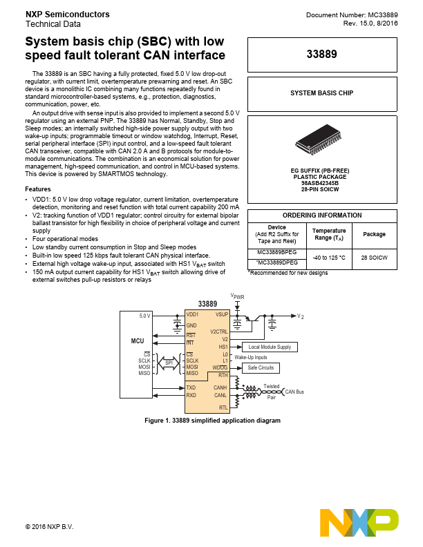
Datasheet4U Logo Datasheet4U.com

MC33889 - System basis chip

General Description

of each pin can be found in the Functional pin description section page 20.

Table 2.

Key Features

  • VDD1: 5.0 V low drop voltage regulator, current limitation, overtemperature detection, monitoring and reset function with total current capability 200 mA.
  • V2: tracking function of VDD1 regulator; control circuitry for external bipolar ballast transistor for high flexibility in choice of peripheral voltage and current supply.
  • Four operational modes.
  • Low standby current consumption in Stop and Sleep modes.
  • Built-in low speed 125 kbps fault tolerant CAN.

📥 Download Datasheet

Full PDF Text Transcription (Reference)

The following content is an automatically extracted verbatim text from the original manufacturer datasheet and is provided for reference purposes only.

View original datasheet text
NXP Semiconductors Technical Data System basis chip (SBC) with low speed fault tolerant CAN interface Document Number: MC33889 Rev. 15.0, 8/2016 33889 The 33889 is an SBC having a fully protected, fixed 5.0 V low drop-out regulator, with current limit, overtemperature prewarning and reset. An SBC device is a monolithic IC combining many functions repeatedly found in standard microcontroller-based systems, e.g., protection, diagnostics, communication, power, etc. An output drive with sense input is also provided to implement a second 5.0 V regulator using an external PNP.