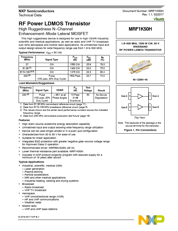
MRF1K50H
Key Features
- High drain--source avalanche energy absorption capability
- Unmatched input and output allowing wide frequency range utilization
- Device can be used single--ended or in a push--pull configuration
- Characterized from 30 to 50 V for ease of use
- Suitable for linear application
- Integrated ESD protection with greater negative gate--source voltage range
- Remended driver: MRFE6VS25N (25 W)
- Lower minimum of 15 years after launch
Applications
- Industrial, scientific, medical (ISM) – Laser generation – Plasma etching – Particle accelerators – MRI and other medical applications – Industrial heating, welding and drying systems