NXP Semiconductors OM6206U
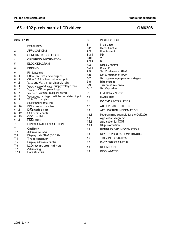
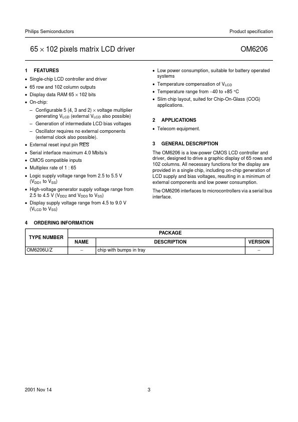
the OM6206 Application diagrams Application for COG Chip information BONDING PAD INFORMATION DEVICE PROTECTION CIRCUITS TRAY INFORMATION DATA SHEET STATUS DEFINITIONS DISCLAIMERS 2001 Nov 14 2 Philips Semiconductors Product specification 65 × 102 pixels matrix LCD driver 1 FEATURES OM6206 • Low power consumption, suitable for battery operated systems • Temperature compensation of VLCD • Temperature range from −40 to +85 °C • Slim chip layout, suited for Chip-On-Glass (COG) applications.| Part No. | OM6206U |
|---|---|
| Datasheet | OM6206U Download |
| Manufacturer |  NXP Semiconductors |
| Description | 65 X 102 pixels matrix LCD driver |
| Buy | Stock & Price |
FEATURES
APPLICATIONS
GENERAL DESCRIPTION
ORDERING INFORMATION BLOCK DIAGRAM PINNING Pin functions R0 to R64: row driver outputs C0 to C101: column driver outputs VSS1 and VSS2: ground supply rails VDD1, VDD2 and VDD3: supply voltage rails VLCDIN: LCD supply voltage VLCDOUT: voltage multiplier output VLCDSENSE: voltage multiplier regulation input T1 to T5: test pins SDIN: serial data line SCLK: serial clock line D/C: mode select SCE: chip enable OSC: oscillator RES: reset FUNCTIONALDESCRIPTION
Oscillator Address counter Display data RAM (DDRAM) Timing generator Display address counter LCD row and column drivers Addressing Data structure 8 8.1 8.2 8.3 8.3.1 8.3.2 8.3.3 8.4 8.4.1 8.5 8.6 8.7 8.8 8.9 8.10 9 10 11 12 13 13.1 13.2 13.3 13.4 14 15 16 17 18 19 INSTRUCTIONS OM6206 Initialization Reset function Function set PD V H Display control D and E Set Y-address of RAM Set X-address of RAM Set high-voltage generator stages Bias system Temperature control Set VOP value LIMITING VALUES HAN...