PCA5007 Description
BLOCK DIAGRAM PINNING FUNCTIONAL DESCRIPTION General CPU timing Overview on the different clocks used within the PCA5007 Memory organization Addressing I/O facilities Timer/event counters I2C-bus serial I/O Serial interface SIO0: SPECIAL MODES OF THE PCA5007 Overview OTP parallel programming mode Test modes APPENDIX 2: THE PARALLEL PROGRAMMING MODE Introduction General description Entering the parallel programming...
PCA5007 Applications
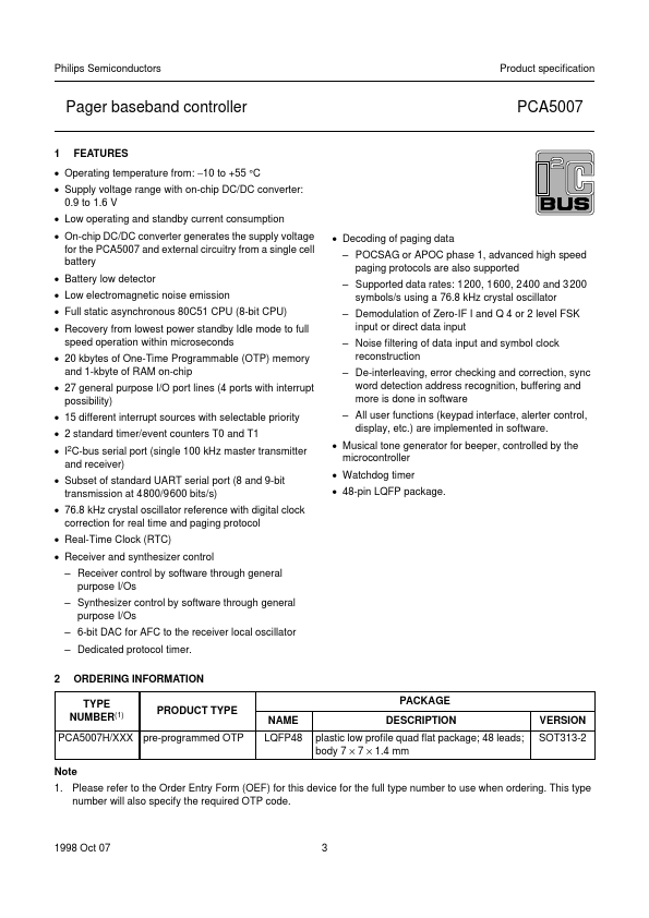
- Operating temperature from: −10 to +55 °C
- Supply voltage range with on-chip DC/DC converter: 0.9 to 1.6 V