DESCRIPTION
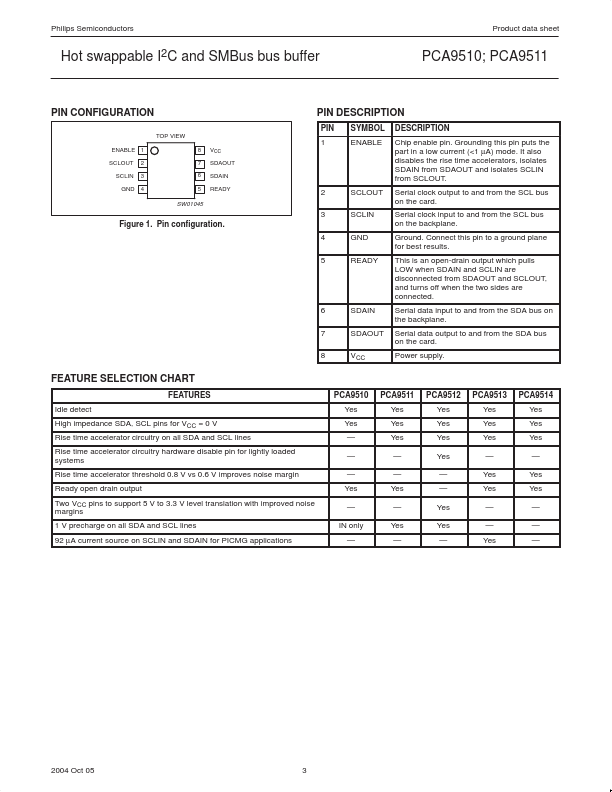
Control circuitry prevents the backplane from being connected to the card until a stop command or bus idle occurs on the backplane without bus contention on the card. The PCA9510 and PCA9511 incorporate a digital ENABLE input pin, which enables the device when asserted HIGH and forces the device into a low current mode when asserted LOW, and an open-drain READY output pin, which indicates that the backplane and card sides are connected together (HIGH) or not (LOW). During insertion, the PCA9510 (IN only) and PCA9511 SDA and SCL lines are precharged to 1 V to minimize the current required to charge the parasitic capacitance of the chip. The dynamic offset design of the PCA9510/11/12/13/14 I/O drivers allow them to be connected to another PCA9510/11/12/13/14 device in series or in parallel and to the A side of the PCA9517. The PCA9510/11/12/13/14 can not connect to the static offset I/Os used on the PCA9515/15A/16/16A/17 B side and PCA9518. FEATURES
● Bi-directional buffer fo... NXP Semiconductors