Datasheet Summary
Low power clock and calendar
Rev. 5
- 24 January 2020
Product data sheet
1. General description
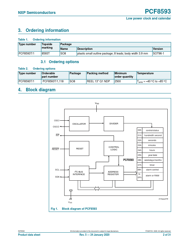
The PCF8593 is a CMOS1 clock and calendar circuit, optimized for low power consumption. Addresses and data are transferred serially via the two-line bidirectional I2C-bus. The built-in word address register is incremented automatically after each written or read data byte. The built-in 32.768 kHz oscillator circuit and the first 8 bytes of the RAM are used for the clock, calendar, and counter functions. The next 8 bytes can be programmed as alarm registers or used as free RAM space.
2. Features and benefits
- I2C-bus interface operating supply voltage: 2.5 V to 6.0 V
- Clock operating...