Datasheet Summary
INTEGRATED CIRCUITS
DATA SHEET
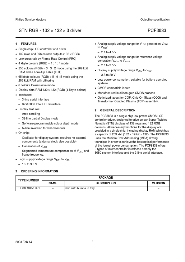
PCF8833 STN RGB
- 132 × 132 × 3 driver
Objective specification 2003 Feb 14
Philips Semiconductors
Objective specification
STN RGB
- 132 × 132 × 3 driver
CONTENTS 1 2 3 4 5 6 6.1 6.2 7 7.1 7.2 7.3 7.4 7.5 7.6 7.7 7.8 7.9 7.10 8 8.1 9 9.1 9.2 Features
GENERAL DESCRIPTION ORDERING INFORMATION BLOCK DIAGRAM PINNING INSTRUCTIONS Exit mands Function set FUNCTIONAL DESCRIPTION MPU interfaces Display data RAM and access arbiter mand decoder Grey scale controller Timing generator Oscillator Reset LCD voltage generator and bias level generator Column drivers, data processing and data latches Row drivers PARALLEL INTERFACE 8080-series 8-bit parallel interface...