PDTC143XT
PDTC143XT is NPN resistor-equipped transistor manufactured by NXP Semiconductors.
URES
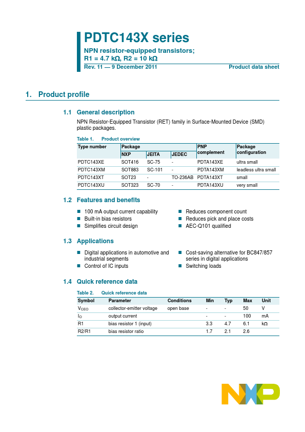
- Built-in bias resistors R1 and R2 (typ. 4.7 kΩ and 10 kΩ respectively)
- Simplification of circuit design
- Reduces number of ponents and board space. APPLICATIONS
- Especially suitable for space reduction in interface and driver circuits
- Inverter circuit configurations without use of external resistors. DESCRIPTION NPN resistor-equipped transistor in a SOT23 plastic package. PINNING PIN 1 2 3 DESCRIPTION base/input emitter/ground collector/output Fig.2 Equivalent inverter symbol.
1 2
MGA893
- 1
PDTC143XT handbook, 4 columns
3 3 R1 1 R2 2 1 2
MAM097
Top view
Fig.1 Simplified outline (SOT23) and symbol.
MARKING TYPE NUMBER
MARKING CODE(1) ∗32
PDTC143XT Note
1. ∗ = p: Made in Hong Kong. ∗ = t: Made in Malaysia.
LIMITING VALUES In accordance with the Absolute Maximum Rating System (IEC 134). SYMBOL VCBO VCEO VEBO VI PARAMETER collector-base voltage collector-emitter voltage emitter-base voltage input voltage positive negative IO ICM Ptot Tstg Tj Tamb Note 1. Refer to SOT23 standard mounting conditions. 1999 Apr 20 2 output current (DC) peak collector current total power dissipation storage temperature junction temperature operating ambient temperature Tamb ≤ 25 °C; note 1
- -
- -
- - 65
- - 65 20
- 7 100 100 250 +150 150 +150 V V m A m A m W °C °C °C CONDITIONS open emitter open base open collector
- -
- MIN. MAX. 50 50 10 V V V UNIT
Philips Semiconductors
Product specification
NPN resistor-equipped transistor
THERMAL CHARACTERISTICS SYMBOL Rth j-a Note 1. Refer to SOT23 standard mounting conditions. CHARACTERISTICS Tamb = 25 °C unless otherwise specified. SYMBOL ICBO ICEO IEBO h FE VCEsat Vi(off) Vi(on) R1 R2 ------R1 Cc PARAMETER collector cut-off current collector cut-off current emitter cut-off current DC current gain collector-emitter saturation voltage input-off voltage input-on voltage input resistor resistor ratio collector capacitance IE = ie = 0; VCB = 10 V; f = 1 MHz CONDITIONS IE = 0; VCB = 50 V IB = 0; VCE = 30 V IB = 0; VCE = 30 V; Tj =...