PHB45NQ10T
PHB45NQ10T is N-channel TrenchMOS transistor manufactured by NXP Semiconductors.
FEATURES
- ’Trench’ technology
- Very low on-state resistance
- Fast switching
- Low thermal resistance
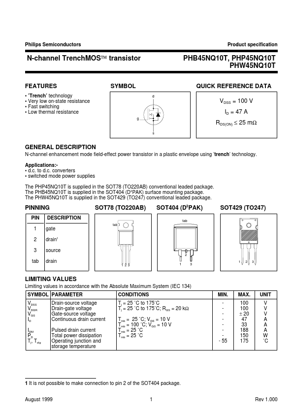
SYMBOL
VDSS = 100 V ID = 47 A g
RDS(ON) ≤ 25 mΩ s
GENERAL DESCRIPTION
N-channel enhancement mode field-effect power transistor in a plastic envelope using ’trench’ technology. Applications:- d.c. to d.c. converters
- switched mode power supplies The PHP45NQ10T is supplied in the SOT78 (TO220AB) conventional leaded package. The PHB45NQ10T is supplied in the SOT404 (D2PAK) surface mounting package. The PHW45NQ10T is supplied in the SOT429 (TO247) conventional leaded package.
PINNING
PIN 1 2 3 tab DESCRIPTION
SOT78 (TO220AB) tab
SOT404 (D2PAK) tab
SOT429 (TO247) gate drain1 source
2 drain
1 23
LIMITING VALUES
Limiting values in accordance with the Absolute Maximum System (IEC 134) SYMBOL PARAMETER VDSS VDGR VGS ID IDM PD Tj, Tstg Drain-source voltage Drain-gate voltage Gate-source voltage Continuous drain current Pulsed drain current Total power dissipation Operating junction and storage temperature CONDITIONS Tj = 25 ˚C to 175˚C Tj = 25 ˚C to 175˚C; RGS = 20 kΩ Tmb = 25 ˚C; VGS = 10 V Tmb = 100 ˚C; VGS = 10 V Tmb = 25 ˚C Tmb = 25 ˚C MIN.
- 55 MAX. 100 100 ± 20 47 33 188 150 175 UNIT V V V A A A W ˚C
1 It is not possible to make connection to pin 2 of the SOT404 package. August 1999 1 Rev 1.000
Philips Semiconductors
Product specification
N-channel Trench MOS™ transistor
PHB45NQ10T, PHP45NQ10T PHW45NQ10T
AVALANCHE ENERGY LIMITING VALUES
Limiting values in accordance with the Absolute Maximum System (IEC 134) SYMBOL PARAMETER EAS Non-repetitive avalanche energy Non-repetitive avalanche current CONDITIONS Unclamped inductive load, IAS = 40 A; tp = 100 µs; Tj prior to avalanche = 25˚C; VDD ≤ 25 V; RGS = 50 Ω; VGS = 10 V; refer to fig:15 MIN. MAX. 260 UNIT m J
- 47
THERMAL RESISTANCES
SYMBOL PARAMETER Rth j-mb Rth j-a Thermal resistance junction to mounting base Thermal resistance junction to ambient CONDITIONS MIN. SOT78...