PHW35NQ20T
PHW35NQ20T is N-channel TrenchMOS transistor manufactured by NXP Semiconductors.
Philips Semiconductors
Product specification
N-channel Trench MOS™ transistor
Features
- ’Trench’ technology
- Very low on-state resistance
- Fast switching
- Low thermal resistance
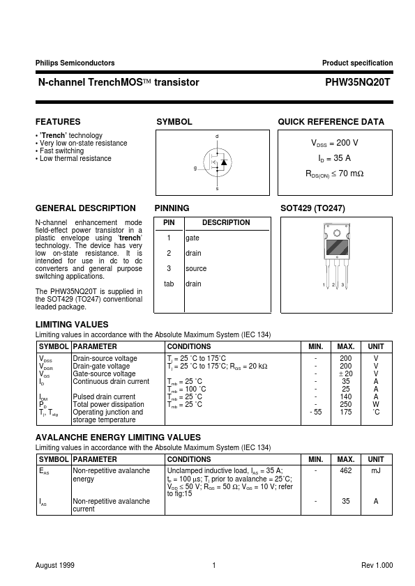
SYMBOL d
QUICK REFERENCE DATA VDSS = 200 V ID = 35 A g
RDS(ON) ≤ 70 mΩ s
GENERAL DESCRIPTION
N-channel enhancement mode field-effect power transistor in a plastic envelope using ’trench’ technology. The device has very low on-state resistance. It is intended for use in dc to dc converters and general purpose switching applications. The PHW35NQ20T is supplied in the SOT429 (TO247) conventional leaded package.
PINNING
PIN 1 2 3 tab gate drain source drain DESCRIPTION
SOT429 (TO247)
LIMITING VALUES
Limiting values in accordance with the Absolute Maximum System (IEC 134) SYMBOL PARAMETER VDSS VDGR VGS ID IDM PD Tj, Tstg Drain-source voltage Drain-gate voltage Gate-source voltage Continuous drain current Pulsed drain current Total power dissipation Operating junction and storage temperature CONDITIONS Tj = 25 ˚C to 175˚C Tj = 25 ˚C to 175˚C; RGS = 20 kΩ Tmb = 25 ˚C Tmb = 100 ˚C Tmb = 25 ˚C Tmb = 25 ˚C MIN.
- 55 MAX. 200 200 ± 20 35 25 140 250 175 UNIT V V V A A A W ˚C
AVALANCHE ENERGY LIMITING VALUES
Limiting values in accordance with the Absolute Maximum System (IEC 134) SYMBOL PARAMETER EAS Non-repetitive avalanche energy Non-repetitive avalanche current CONDITIONS Unclamped inductive load, IAS = 35 A; tp = 100 µs; Tj prior to avalanche = 25˚C; VDD ≤ 50 V; RGS = 50 Ω; VGS = 10 V; refer to fig:15 MIN. MAX. 462 UNIT m J
- 35
August 1999
Rev 1.000
Philips Semiconductors
Product specification
N-channel Trench MOS™ transistor
THERMAL RESISTANCES
SYMBOL PARAMETER Rth j-mb Rth j-a Thermal resistance junction to mounting base Thermal resistance junction to ambient CONDITIONS TYP. in free air 45 MAX. 0.6 UNIT K/W K/W
ELECTRICAL CHARACTERISTICS...