PIP3118-B
PIP3118-B is LOGIC LEVEL TOPFET manufactured by NXP Semiconductors.
DESCRIPTION
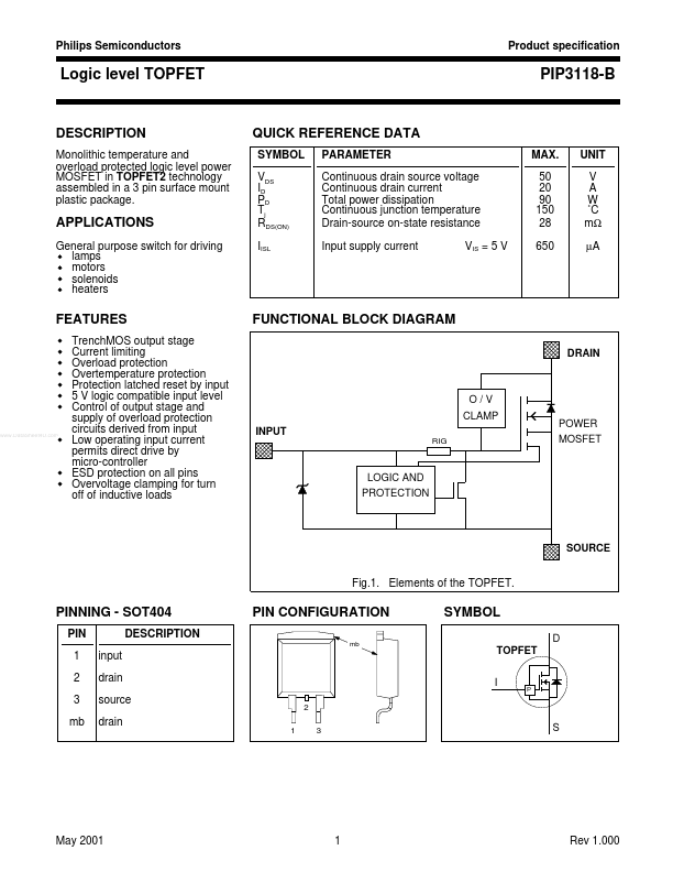
Monolithic temperature and overload protected logic level power MOSFET in TOPFET2 technology assembled in a 3 pin surface mount plastic package.
QUICK REFERENCE DATA
SYMBOL VDS ID PD Tj RDS(ON) IISL PARAMETER Continuous drain source voltage Continuous drain current Total power dissipation Continuous junction temperature Drain-source on-state resistance Input supply current VIS = 5 V MAX. 50 20 90 150 28 650 UNIT V A W ˚C mΩ µA
APPLICATIONS
General purpose switch for driving lamps motors solenoids heaters
FEATURES
Trench MOS output stage Current limiting Overload protection Overtemperature protection Protection latched reset by input 5 V logic patible input level Control of output stage and supply of overload protection circuits derived from input Low operating input current permits direct drive by micro-controller ESD protection on all pins Overvoltage clamping for turn off of inductive loads
FUNCTIONAL BLOCK DIAGRAM
DRAIN
O/V CLAMP INPUT
POWER MOSFET
..
LOGIC AND PROTECTION
SOURCE
Fig.1. Elements of the TOPFET.
PINNING
- SOT404
PIN 1 2 3 mb input drain source drain DESCRIPTION
PIN CONFIGURATION mb
SYMBOL
D TOPFET I
2 1 3
May 2001
Rev 1.000
Philips Semiconductors
Product specification
Logic level TOPFET
LIMITING VALUES
Limiting values in accordance with the Absolute Maximum Rating System (IEC 134) SYMBOL VDS ID ID II IIRM PD Tstg Tj Tsold PARAMETER Continuous drain source voltage Continuous drain current
CONDITIONS VIS = 5 V; Tmb = 25˚C VIS = 5 V; Tmb ≤ 121˚C δ ≤ 0.1, tp = 300 µs Tmb ≤ 25˚C normal operation during soldering
MIN. -5 -50 -55
- MAX. 50 self limited 20 5 50 90 175 150 260
UNIT V A A m A m A W ˚C ˚C ˚C
Continuous drain current Continuous input current Repetitive peak input current Total power dissipation Storage temperature Continuous junction temperature2 Case...