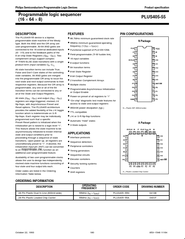
Datasheet4U Logo Datasheet4U.com
NXP Semiconductors logo

PLUS405-55

Manufacturer: NXP Semiconductors

PLUS405-55 datasheet by NXP Semiconductors.

PLUS405-55 datasheet preview

PLUS405-55 Datasheet Details

Part number PLUS405-55
Datasheet PLUS405-55_PhilipsSemiconductors.pdf
File Size 166.03 KB
Manufacturer NXP Semiconductors
Description Programmable logic sequencer
PLUS405-55 page 2 PLUS405-55 page 3

PLUS405-55 Overview

The PLUS405-55 device is a bipolar, programmable state machine of the Mealy type. Both the AND and the OR array are user-programmable. All 64 AND gates are connected to the 16 external dedicated inputs (I0 - I15) and to the feedback paths of the 8 on-chip State Registers (QP0 - QP7).

PLUS405-55 Key Features

  • 66.7MHz minimum guaranteed clock rate
  • 55MHz minimum guaranteed operating
  • Functional superset of PLS105/105A
  • Field-programmable (Ti-W fusible link)
  • 16 input variables
  • 8 output functions
  • 64 transition terms
  • 8-bit State Register
  • 8-bit Output Register
  • 2 transition plement Arrays
NXP Semiconductors logo - Manufacturer

More Datasheets from NXP Semiconductors

View all NXP Semiconductors datasheets

Part Number Description
PLUS105-45 Programmable logic sequencer
PLUS153B Programmable logic arrays
PLUS153D Programmable logic arrays
PLUS16L4D PAL devices
PLUS16L6D PAL devices
PLUS16L8D PAL devices
PLUS16R4D PAL devices
PLUS16R6D PAL devices
PLUS16R8D PAL devices
PLUS173-10 Programmable logic array

PLUS405-55 Distributor

Datasheet4U Logo
Since 2006. D4U Semicon. About Datasheet4U Contact Us Privacy Policy Purchase of parts