Download PSMN7R6-100BSE Datasheet PDF
NXP Semiconductors
PSMN7R6-100BSE
PSMN7R6-100BSE is N-channel MOSFET manufactured by NXP Semiconductors.
description 
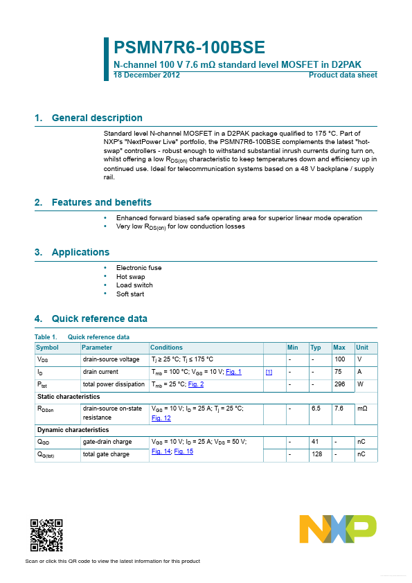
Standard level N-channel MOSFET in a D2PAK package qualified to 175 °C. Part of NXP's "Next Power Live" portfolio, the PSMN7R6-100BSE plements the latest "hotswap" controllers - robust enough to withstand substantial inrush currents during turn on, whilst offering a low RDS(on) characteristic to keep temperatures down and efficiency up in continued use. Ideal for telemunication systems based on a 48 V backplane / supply rail. 2. Features and benefits - - Enhanced forward biased safe operating area for superior linear mode operation Very low RDS(on) for low conduction losses 3. Applications - - - - Electronic fuse Hot swap Load switch Soft start 4. Quick reference data Table 1. Symbol VDS ID Ptot RDSon Quick reference data Parameter drain-source voltage drain current total power dissipation Conditions Tj ≥ 25 °C; Tj ≤ 175 °C Tmb = 100 °C; VGS = 10 V; Fig. 1 Tmb = 25 °C; Fig. 2 VGS = 10 V; ID = 25 A; Tj = 25 °C; Fig. 12 VGS = 10 V; ID = 25 A; VDS = 50 V; Fig. 14; Fig. 15 41 128 n C n C [1] Min - Typ - Max 100 75 296 Unit V A W Static characteristics drain-source on-state resistance 6.5 7.6 mΩ Dynamic characteristics QGD QG(tot) gate-drain charge total gate charge Scan or click this QR code to view the latest information for this product Free Datasheet http://..net/ NXP Semiconductors N-channel 100 V 7.6 mΩ standard level MOSFET in D2PAK Symbol EDS(AL)S Parameter non-repetitive drainsource avalanche energy [1] Conditions VGS = 10 V; Tj(init) = 25 °C; ID = 75 A; Vsup ≤ 100 V; RGS = 50 Ω; unclamped; Fig. 3 Min - Typ - Max 426 Unit m J Avalanche Ruggedness Continuous current limited by package 5. Pinning information Table 2. Pin 1 2 3 mb Pinning information Symbol Description G D S D gate drain[1] source mounting base; connected to drain 2 1 3 G mbb076 Simplified outline mb Graphic...