NXP Semiconductors SSTL16877
The SSTL16877 is a 14-bit SSTL_2 registered driver with differential clock inputs, designed to operate between 2.3 V and 2.7 V. The outputs support class I which can be used for standard stub-series applications or capacitive loads. The SSTL16877 is intended to be incorporated into standard DIMM (Dual In-Line Memory Module) designs defined by JEDEC, such as DDR (Double Data Rate) SDRAM or SDRAM II Memory Modules.| Part No. | SSTL16877 |
|---|---|
| Datasheet | SSTL16877 Download |
| Manufacturer |  NXP Semiconductors |
| Description | 14-bit SSTL_2 registered driver |
| Buy | Stock & Price |
FEATURES
● Stub-series terminated logic for 2.5 V VDDQ (SSTL_2)● Optimized for DDR (Double Data Rate) SDRAM applications
● Supports SSTL_2 signal inputs and outputs
● Flow-through architecture optimizes PCB layout
● Meets SSTL_2 class I and class II specifications
● Latch-up protection exceeds 500mA per JEDEC Std 17
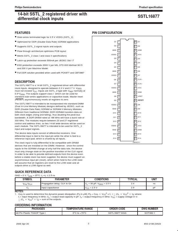
● ESD protection exceeds 2000 V per MIL STD 833 Method 3015 and 200 V per Machine Model PIN CONFIGURATION Q1 Q2 GND VDDQ Q3 Q4 Q5 GND VDDQ 1 2 3 4 5 6 7 8 9 48 D1 47 D2 46 GND 45 VCC 44 D3 43 D4 42 D5 41 D6 40 D7 39 CLK– 38 CLK+ 37 VCC 36 GND 35 VREF 34 RESET 33 D8 32 D9 31 D10 30 D11 29 D12 28 VCC 27 GND 26 D13 25 D14
● Full DDR solution provided when used with PCK877 and CBT3867
DESCRIPTION
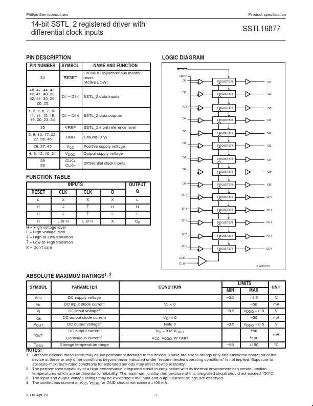
VDDQ must not exceed VCC. Inputs are SSTL_2 type with VREF normally at 0.5*VDDQ. Master reset (RESET) asynchronously resets all registers to zero. Different from traditional SDRAM, DDR SDRAM transfers data on both clock edges (rising and falling), thus doubling the peak bus bandwidth. A DDR DRAM rated at 166 MHz will have a burst rate of 333 MHz.