NXP Semiconductors TDA4662
The TDA4662 is an integrated baseband delay line circuit with one line delay. It is suitable for PAL and NTSC decoders with colour-difference signal outputs ±(R−Y) and ±(B−Y).| Part No. | TDA4662 |
|---|---|
| Datasheet | TDA4662 Download |
| Manufacturer |  NXP Semiconductors |
| Description | Baseband delay line |
| Buy | Stock & Price |
FEATURES
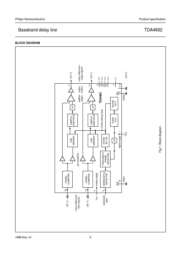
● Two comb filters, using the switched-capacitor technique, for one line delay time (64 µs)● For PAL and NTSC
● Adjustment-free application
● Handles negative or positive colour-difference input signals
● Clamping of AC-coupled input signals [±(R−Y) and ±(B−Y)]
● VCO without external components
● 3 MHz internal clock signal derived from a 6 MHz CCO, line-locked by the sandcastle pulse (64 µs line)
● Sample-and-hold circuits and low-pass filters to suppress the 3 MHz clock signal
● Addition of delayed and non-delayed output signals
● Output buffer amplifiers
● Comb filtering functions for NTSC colour-difference signals to suppress cross-colour. QUICK REFERENCE DATA SYMBOL VP1 VP2 IP(tot) Vi(p-p) Gv PARAMETER analog supply voltage (pin 9) digital supply voltage (pin 1) total supply current MIN. 4.5 4.5 − 5 5 5.5 525 665 5.8 5.8 TYP. 6 6
GENERAL DESCRIPTION
TDA4662 MAX. V V UNIT 7.0 − − 6.3 6.3 mA mV mV dB dB ±(R−Y) input signal PAL/NTSC (peak-to-peak value; pin 16) − ±(B−Y) inp...