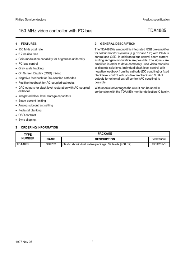
FEATURES
GENERAL DESCRIPTION
ORDERING INFORMATION QUICK REFERENCE DATA BLOCK DIAGRAM PINNING FUNCTIONAL DESCRIPTION
Signal input stage (input clamping, blanking and clipping) Electronic potentiometer stages Contrast control (driven by I2C-bus, 6-bit DAC) Brightness control (driven by I2C-bus, 6-bit DAC) Gain control (driven by I2C-bus, 6-bit DAC) and grey scale tracking Output stage Pedestal blanking Output clamping, feedback references and DAC outputs Clamping and blanking pulses On Screen Display (OSD) Limiting by contrast reduction Gain modulation I2C-bus control LIMITING VALUES THERMAL CHARACTERISTICS CHARACTERISTICS I2C-BUS PROTOCOL INTERNAL CIRCUITRY TEST AND APPLICATION INFORMATION Test application Recommendations for building the application board PACKAGE OUTLINE SOLDERING Introduction Soldering by dipping or by wave Repairing soldered joints DEFINITIONS LIFE SUPPORT APPLICATIONS
PURCHASE OF PHILIPS I2C COMPONENTS TDA4885 1997 Nov 25 2 Philips Semiconductors Product specificatio... NXP Semiconductors