Datasheet4U Logo Datasheet4U.com

TDA8792 - 3.3 V/ 25 MHz 8-bit analog-to-digital converter ADC

Description

The TDA8792 is a 8-bit analog-to-digital converter (ADC) for low-voltage, portable applications.

It operates at 3.3 V and converts the analog input signal into 8-bit binary-coded digital words at a maximum sampling rate of 25 MHz.

The output data is valid after a delay of 6 clock cycles.

Features

  • 8-bit resolution.
  • Sampling rate up to 25 MHz.
  • 30 MHz input signal bandwidth (full scale).
  • High signal-to-noise ratio over a large analog input frequency range (7.3 effective bits at 4.43 MHz full-scale input at fclk = 25 MHz).
  • CMOS compatible digital inputs.
  • External reference voltage regulator.
  • Power dissipation only 53 mW (typical).
  • Standby mode (only 1.2 mW typical).
  • Low analog input capacitance, no buffer ampli.

📥 Download Datasheet

Datasheet preview – TDA8792

Datasheet Details

Part number TDA8792
Manufacturer NXP
File Size 148.99 KB
Description 3.3 V/ 25 MHz 8-bit analog-to-digital converter ADC
Datasheet download datasheet TDA8792 Datasheet
Additional preview pages of the TDA8792 datasheet.
Other Datasheets by NXP

Full PDF Text Transcription

Click to expand full text
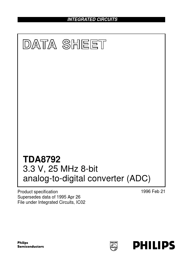
INTEGRATED CIRCUITS DATA SHEET TDA8792 3.3 V, 25 MHz 8-bit analog-to-digital converter (ADC) Product specification Supersedes data of 1995 Apr 26 File under Integrated Circuits, IC02 1996 Feb 21 Philips Semiconductors Product specification 3.3 V, 25 MHz 8-bit analog-to-digital converter (ADC) FEATURES • 8-bit resolution • Sampling rate up to 25 MHz • 30 MHz input signal bandwidth (full scale) • High signal-to-noise ratio over a large analog input frequency range (7.3 effective bits at 4.43 MHz full-scale input at fclk = 25 MHz) • CMOS compatible digital inputs • External reference voltage regulator • Power dissipation only 53 mW (typical) • Standby mode (only 1.2 mW typical) • Low analog input capacitance, no buffer amplifier required • No sample-and-hold circuit required.
Published: |