NXP Semiconductors TDA8927
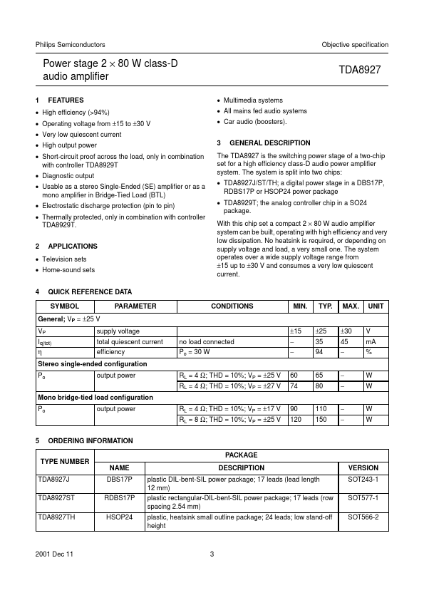
The TDA8927 is the switching power stage of a two-chip set for a high efficiency class-D audio power amplifier system. The system is split into two chips: • TDA8927J/ST/TH; a digital power stage in a DBS17P, RDBS17P or HSOP24 power package • TDA8929T; the analog controller chip in a SO24 package. With this chip set a compact 2 × 80 W audio amplifier system can be built, operating with high efficiency and very low dissipation.| Part No. | TDA8927 |
|---|---|
| Datasheet | TDA8927 Download |
| Manufacturer |  NXP Semiconductors |
| Description | Power stage 2 x 80 W class-D audio amplifier |
| Buy | Stock & Price |
FEATURES
APPLICATIONS
GENERAL DESCRIPTION
QUICK REFERENCE DATA ORDERING INFORMATION BLOCK DIAGRAMS PINNING INFORMATION FUNCTIONALDESCRIPTION
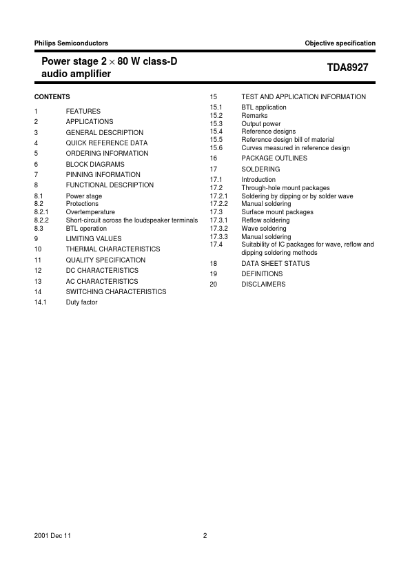
Power stage Protections Overtemperature Short-circuit across the loudspeaker terminals BTL operation LIMITING VALUES THERMAL CHARACTERISTICS QUALITY SPECIFICATION DC CHARACTERISTICS AC CHARACTERISTICS SWITCHING CHARACTERISTICS Duty factor 15 15.1 15.2 15.3 15.4 15.5 15.6 16 17 17.1 17.2 17.2.1 17.2.2 17.3 17.3.1 17.3.2 17.3.3 17.4 18 19 20 TDA8927 TEST AND APPLICATION INFORMATION BTL application Remarks Output power Reference designs Reference design bill of material Curves measured in reference design PACKAGE OUTLINES SOLDERING Introduction Through-hole mount packages Soldering by dipping or by solder wave Manual soldering Surface mount packages Reflow soldering Wave soldering Manual soldering Suitability of IC packages for wave, reflow and dipping soldering methods DATA SHEET STATUS DEFINITIONS DISCLAIMERS 2001 Dec 11 2 Philips Semiconductors O...