NXP Semiconductors TDA9177
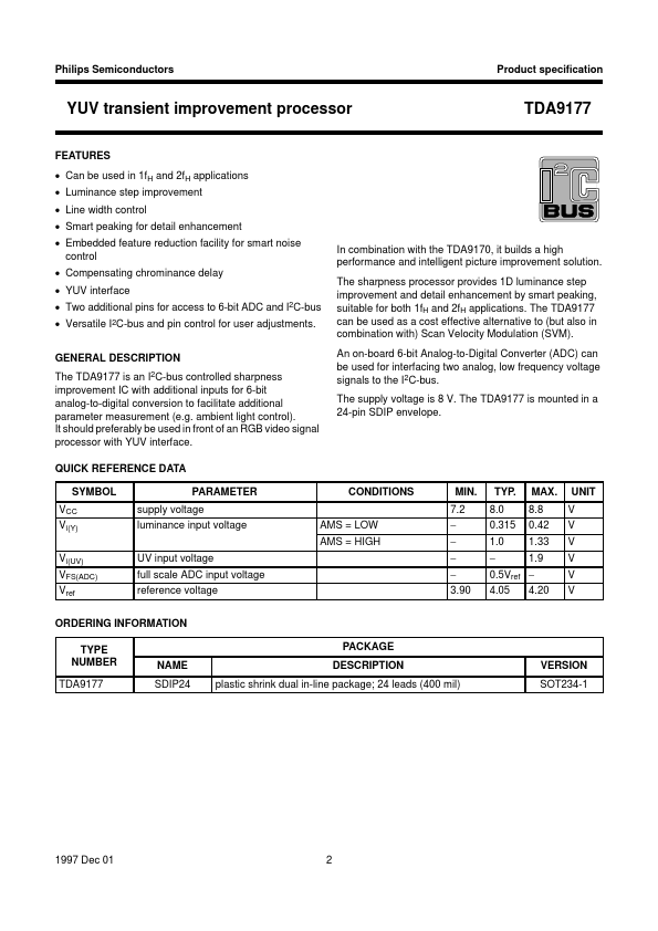
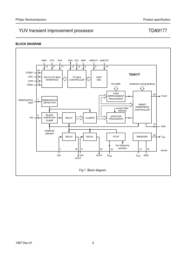
The TDA9177 is an I2C-bus controlled sharpness improvement IC with additional inputs for 6-bit analog-to-digital conversion to facilitate additional parameter measurement (e.g. It should preferably be used in front of an RGB video signal processor with YUV interface. The TDA9177 can be used as a cost effective alternative to (but also in combination with) Scan Velocity Modulation (SVM).| Part No. | TDA9177 |
|---|---|
| Datasheet | TDA9177 Download |
| Manufacturer |  NXP Semiconductors |
| Description | YUV transient improvement processor |
| Buy | Stock & Price |
FEATURES
● Can be used in 1fH and 2fH applications● Luminance step improvement
● Line width control
● Smart peaking for detail enhancement
● Embedded feature reduction facility for smart noise control
● Compensating chrominance delay
● YUV interface
● Two additional pins for access to 6-bit ADC and I2C-bus
● Versatile I2C-bus and pin control for user adjustments.
GENERAL DESCRIPTION
ambient light control). QUICK REFERENCE DATA SYMBOL VCC Vi(Y) Vi(UV) VFS(ADC) Vref PARAMETER supply voltage luminance input voltage UV input voltage full scale ADC input voltage reference voltage AMS = LOW AMS = HIGH CONDITIONS MIN. 7.2 − − − − 3.90 TYP. 8.0 0.315 1.0 − 4.05 TDA9177 In combination with the TDA9170, it builds a high performance and intelligent picture improvement solution. The sharpness processor provides 1D luminance step improvement and detail enhancement by smart peaking, suitable for both 1fH and 2fH applications. An on-board 6-bit Analog-to-Digital Converter (ADC) can be used for interfacing two analog, low frequency voltage signals to the I2C-bus.