Datasheet4U Logo Datasheet4U.com

VR5100 - Multi-output DC/DC regulator

Datasheet Summary

Description

.

.

.

Features

  • Three adjustable high efficiency buck regulators: 3.8 A, 1.25 A, 1.5 A.
  • Selectable modes: PWM, PFM, APS.
  • 5.0 V, 600 mA boost regulator with PFM or Auto mode.
  • Six adjustable general purpose linear regulators.
  • Input voltage range: 2.8 V to 4.5 V.
  • OTP (One Time Programmable) memory for device configuration.
  • Programmable start-up sequence and timing.
  • Selectable output voltage, frequency, soft start.
  • I2C control.

📥 Download Datasheet

Datasheet preview – VR5100

Datasheet Details

Part number VR5100
Manufacturer NXP
File Size 2.79 MB
Description Multi-output DC/DC regulator
Datasheet download datasheet VR5100 Datasheet
Additional preview pages of the VR5100 datasheet.
Other Datasheets by NXP

Full PDF Text Transcription

Click to expand full text
NXP Semiconductors Data sheet: Advance Information Multi-output DC/DC regulator for low-power LS1 communication processors Document Number: VR5100 Rev. 5.0, 12/2018 VR5100 
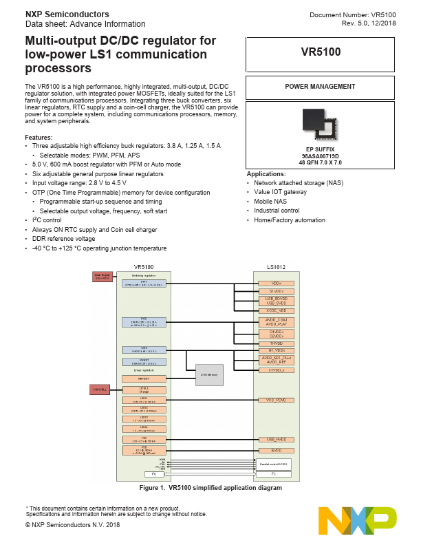
The VR5100 is a high performance, highly integrated, multi-output, DC/DC regulator solution, with integrated power MOSFETs, ideally suited for the LS1 family of communications processors. Integrating three buck converters, six linear regulators, RTC supply and a coin-cell charger, the VR5100 can provide power for a complete system, including communications processors, memory, and system peripherals. POWER MANAGEMENT Features: • Three adjustable high efficiency buck regulators: 3.8 A, 1.25 A, 1.5 A • Selectable modes: PWM, PFM, APS • 5.
Published: |