Datasheet Summary
..
NanoAmp Solutions, Inc. 1982 Zanker Road, San Jose, CA 95112 ph: 408-573-8878, FAX: 408-573-8877 .nanoamp.
N16T1618C2(D1/A1)A
Advance Information
16Mb Ultra-Low Power Asynchronous CMOS PSRAM
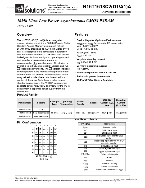
1M x 16 bit Overview
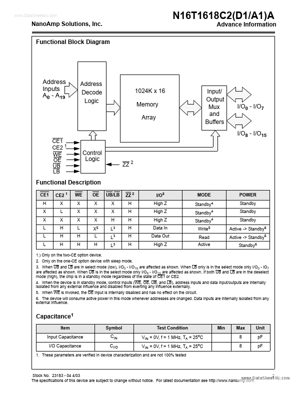
The N16T1618C2(D1/A1)A is an integrated memory device containing a 16 Mbit Pseudo Static Random Access Memory using a self-refresh DRAM array organized as 1,048,576 words by 16 bits. It is designed to be patible in operation and interface to standard 6T SRAMS. The device is designed for low standby and operating current and includes a power-down feature to automatically enter standby mode. The device is available in a 2 CE (chip enable) version and...