Datasheet4U Logo Datasheet4U.com

NT5TU256M4GE - 1Gb DDR2 SDRAM

Description

The 1giga-bit (1Gb) Double-Data-Rate-2 (DDR2) DRAMs is a high-speed CMOS Double Data Rate 2 SDRAM containing 1,073,741,824 bits.

It is internally configured as an octal-bank DRAM.

The 1Gb chip is organized as 32Mbit x 4 I/O x 8 bank, 16Mbit x 8 I/O x 8 bank or 8Mbit x 16 I/O x 8 bank device.

Features

  • (1) posted CAS with additive latency, (2) write latency = read latency -1, (3) normal and weak strength data-output driver, (4) variable data-output impedance adjustment and (5) an ODT (On-Die Termination) function. All of the control and address inputs are synchronized with a pair of externally supplied differential clocks. Inputs are latched at the cross point of differential clocks (CK rising and  falling). All I/Os are synchronized with a single ended DQS or differential DQS pair in a so.

📥 Download Datasheet

Datasheet Details

Part number NT5TU256M4GE
Manufacturer Nanya
File Size 2.34 MB
Description 1Gb DDR2 SDRAM
Datasheet download datasheet NT5TU256M4GE Datasheet
Other Datasheets by Nanya

Full PDF Text Transcription

Click to expand full text
NT5TU256M4GE / NT5TU128M8GE / NT5TU64M16GG 1Gb DDR2 SDRAM Feature 
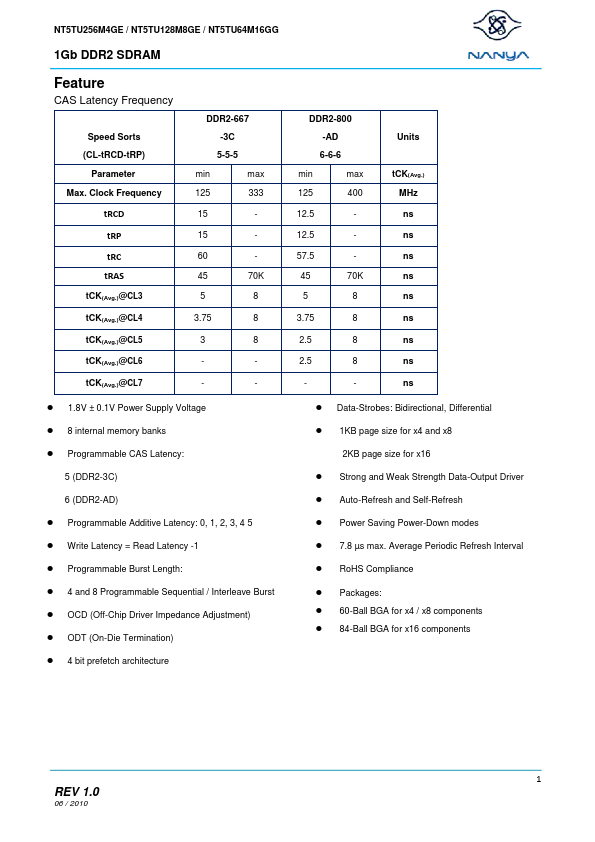
CAS Latency Frequency DDR2-667 Speed Sorts (CL-tRCD-tRP) Parameter Max. Clock Frequency min 125 15 15 60 45 5 3.75 3 -3C 5-5-5 max 333 70K 8 8 8 min 125 12.5 12.5 57.5 45 5 3.75 2.5 2.5   DDR2-800 -AD 6-6-6 max 400 70K 8 8 8 8 tCK(Avg.) MHz ns ns ns ns ns ns ns ns ns Units tRCD tRP tRC tRAS tCK(Avg.)@CL3 tCK(Avg.)@CL4 tCK(Avg.)@CL5 tCK(Avg.)@CL6 tCK(Avg.)@CL7    1.8V ± 0.1V Power Supply Voltage 8 internal memory banks Programmable CAS Latency: 5 (DDR2-3C) 6 (DDR2-AD) Data-Strobes: Bidirectional, Differential 1KB page size for x4 and x8 2KB page size for x16         Strong and Weak Strength Data-Output Driver Auto-Refresh and Self-Refresh Power Saving Power-Down modes 7.8 µs max.
Published: |