Description
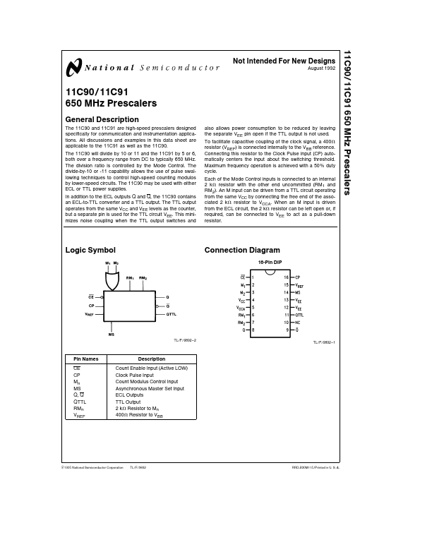
The 11C90 and 11C91 are high-speed prescalers designed specifically for munication and instrumentation applications All discussions and examples in this data sheet are applicable to the 11C91 as well as the 11C90 The 11C90 will divide by 10 or 11 and the 11C91 by 5 or 6 both over a frequency range from DC to typically 650 MHz The division ratio is controlled by the Mode Control The divide-by-10 or -11 capability allows the use of pulse swallowing techniques to control high-speed counting modulos by lower-speed circuits The 11C90 may be used with either ECL or TTL power supplies In addition to the ECL outputs Q and Q the 11C90 contains an ECL-to-TTL converter and a TTL output The TTL output operates from the same VCC and VEE levels as the counter but a separate pin is used for the TTL circuit VEE This minimizes noise coupling when the TTL output switches and also allows power consumption to be reduced by leaving the separate VEE pin open if the TTL output is not used To facilitate capacitive coupling of the clock signal a 400X resistor (VREF) is connected internally to the VBB reference Connecting this resistor to the Clock Pulse input (CP) automatically centers the input about the switching threshold Maximum frequency operation is achieved with a 50% duty cycle Each of the Mode Control inputs is connected to an internal 2 kX resistor with the other end unmitted (RM1 and RM2) An M input can be driven from a TTL circuit operating from the same VCC by connecting the free end of the associated 2 kX resistor to VCCA When an M input is driven from the ECL circuit the 2 kX resistor can be left open or if required can be connected to VEE to act as a pull-down resistor Logic Symbol Connection Diagram 16-Pin DIP Pin Names CE CP Mn MS QQ QTTL RMn VREF TL F 9892 - 2 Description Count Enable Input (Active LOW) Clock Pulse Input Count Modulus Control Input Asynchronous Master Set Input ECL Outputs TTL Output 2 kX Resistor to Mn 400X Resistor to VBB C1995 National Semiconductor Corporation TL F 9892 TL F 9892 - 1 RRD-B30M115 Printed in U S A Above which the useful life may be impaired If Military Aerospace specified devices are required please contact the National Semiconductor Sales Office Distributors for availability and specifications Storage Temperature b65 C to a150 C Maximum Junction Temperature (TJ) Supply Voltage Range a150 C b7 0V to GND Input Voltage (DC) Output Current (DC Output HIGH) VEE to GND b50 mA Operating Range b5 7V to b4 7V Lead Temperature (Soldering 10 sec ) 300 C Remended Operating Conditions Min Typ Ambient Temperature (TA) mercial 0C Military b55 C Supply Voltage (VEE) mercial b5 7V b5 2V Military b5 7V b5 2V Max a75 C a125 C b4 7V b4 7V TTL Input Output Operation DC Over Operating Temperature and Voltage Range unless otherwise noted Pins 12 and 13 e GND Symbol VIH VIL VOH VOL IIL ISC Parameter Input HIGH Voltage M1 and M2 Inputs Input LOW Voltage M1 and M2 Inputs Output HIGH Voltage QTTL Output Output LOW Voltage QTTL Output Input LOW Current M1 and M2 Inputs Output Short Circuit Current Min 23 b20 Typ (Note 3) 41 33 33 02 b2 3 b35 Max 05 b5 0 b80 Units V V V V mA mA Conditions Guaranteed Input HIGH Threshold Voltage (Note 4) VCC e VCCA e 5 0V Guaranteed Input LOW Threshold Voltage (Note 4) VCC e VCCA e 5 0V VCC e VCCA e Min IOH e b640 mA VCC e VCCA e Min IOL e 20 0 mA VCC e VCCA e Max VIN e 0 4V Pins 6 7 e VCC VCC e VCCA e Max VOUT e 0 0V Pin 14 e VCC AC VCC e VCCA e 5 0V Nominal VEE e GND TA e a25 C Symbol Parameter Min Typ Max Units Conditions tPLH tPHL Propagation Delay (50% to 50%) CP to QTTL 6 10 14 ns See Figure 1 tPLH Propagation Delay (50% to 50%) MS to QTTL 12 17 ns ts Mode Control Setup Time 4 2 ns th Mode Control Hold.