GENERAL DESCRIPTION
n Non-inverting TRI-STATE outputs drive bus lines or buffer memory address registers n Outputs source/sink 24 mA n ’ACT241 has TTL-compatible inputs n Standard Microcircuit Drawing (SMD) — ’AC241: 5962-87551 — ’ACT241: 5962-89847 FEATURES
n ICC and IOZ reduced by 50% Logic Symbol Connection Diagrams Pin Assignment for DIP and Flatpak DS100281-1 DS100281-2 Pin Names OE1, OE2 I0–I7 O0–O7 DESCRIPTION
TRI-STATE Output Enable Input TRI-STATE Output Enable Input (Active HIGH) Inputs Outputs Pin Assignment for LCC DS100281-3 TRI-STATE ® is a registered trademark of National Semiconductor Corporation. FACT ® is a registered trademark of Fairchild Semiconductor Corporation. © 1998 National Semiconductor Corporation DS100281 Truth Tables Inputs OE1 L L H Inputs OE2 H H L H = HIGH Voltage Level L = LOW Voltage Level X = Immaterial Z = High Impedance Outputs In L H X (Pins 12, 14, 16, 18) L H Z Outputs In L H X (Pins 3, 5, 7, 9) L H Z 2 ABSOLUTE MAXIMUM RATINGS
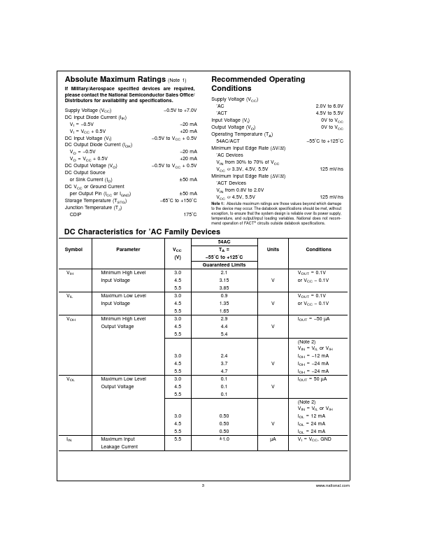
(Note 1) If Mili... National Semiconductor