GENERAL DESCRIPTION
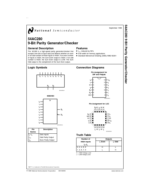
If an even number of inputs is HIGH, the Sum Even output is HIGH. If an odd number is HIGH, the Sum Even output is LOW. FEATURES
n ICC reduced by 50% n 9-bit width for memory applications n Standard Microcircuit Drawing (SMD) 5962-92201 Logic Symbols Connection Diagrams Pin Assignment for DIP and Flatpak DS100359-1 IEEE/IEC DS100359-2 Pin Assignment for LCC DS100359-4 Pin Names I0–I8 ∑O ∑E DESCRIPTION
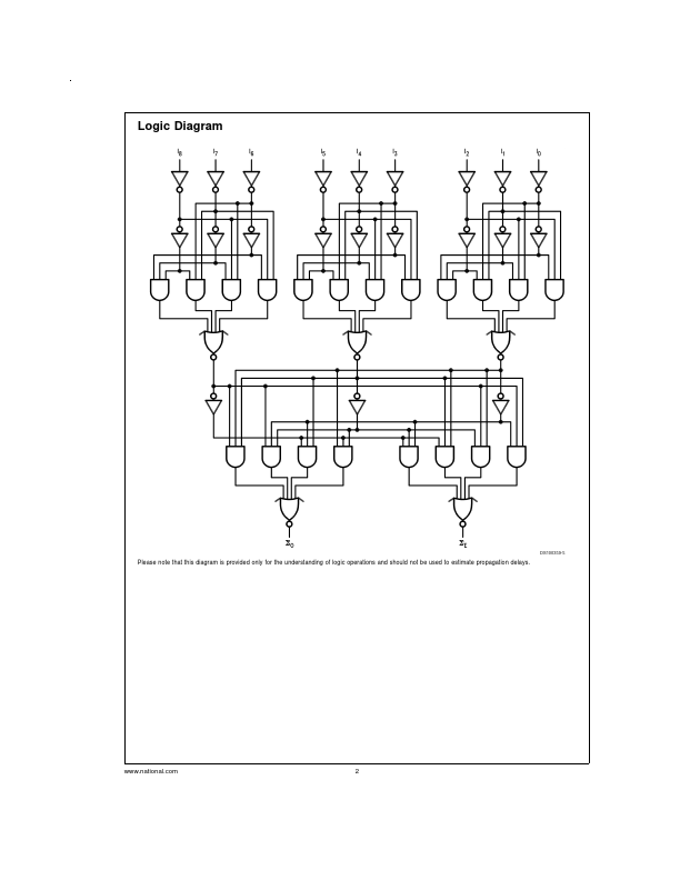
DS100359-3 Data Inputs Odd Parity Output Even Parity Output Truth Table Number of HIGH Inputs I0–I8 0, 2, 4, 6, 8 1, 3, 5, 7, 9 H = HIGH Voltage Level L = LOW Voltage Level Outputs ∑ Even ∑ Odd H L L H FACT™ is a trademark of Fairchild Semiconductor Corporation. © 1998 National Semiconductor Corporation DS100359 Logic Diagram DS100359-5 Please note that this diagram is provided only for the understanding of logic operations and should not be used to estimate propagation delays. 2 ABSOLUTE MAXIMUM RATINGS
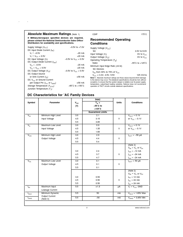
(Note 1) If Military/Aerospace specified devices are required, please contact the National Semiconductor Sales Office/ Distributors for availability and specifications. National Semiconductor