54AC74
54AC74 is Dual D-Type Positive Edge-Triggered Flip-Flop manufactured by National Semiconductor.
..
- 54ACT74 Dual D-Type Positive Edge-Triggered Flip-Flop
August 1998
- 54ACT74 Dual D-Type Positive Edge-Triggered Flip-Flop
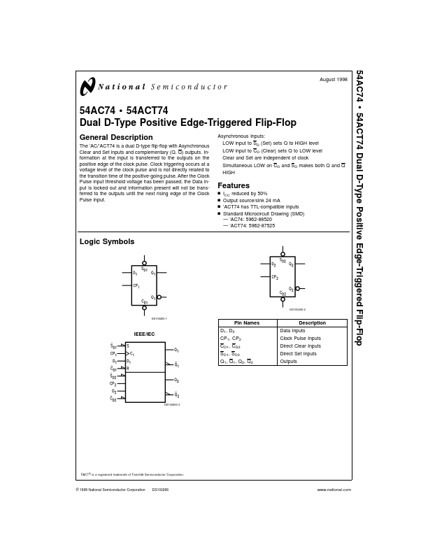
General Description
The ’AC/’ACT74 is a dual D-type flip-flop with Asynchronous Clear and Set inputs and plementary (Q, Q) outputs. Information at the input is transferred to the outputs on the positive edge of the clock pulse. Clock triggering occurs at a voltage level of the clock pulse and is not directly related to the transition time of the positive-going pulse. After the Clock Pulse input threshold voltage has been passed, the Data input is locked out and information present will not be transferred to the outputs until the next rising edge of the Clock Pulse input. Asynchronous Inputs: LOW input to SD (Set) sets Q to HIGH level LOW input to CD (Clear) sets Q to LOW level Clear and Set are independent of clock Simultaneous LOW on CD and SD makes both Q and Q HIGH
Features n n n n ICC reduced by 50% Output source/sink 24 m A ’ACT74 has TTL-patible inputs Standard Microcircuit Drawing (SMD)
- ’AC74: 5962-88520
- ’ACT74: 5962-87525
Logic Symbols
DS100266-2 DS100266-1
Pin Names IEEE/IEC D1, D2 CP1, CP2 CD1, CD2 SD1, SD2 Q1, Q1, Q2, Q2
Description Data Inputs Clock Pulse Inputs Direct Clear Inputs Direct Set Inputs Outputs
DS100266-3
FACT ® is a registered trademark of Fairchild Semiconductor Corporation.
© 1998 National Semiconductor Corporation
DS100266
.national.
Connection Diagrams
Pin Assignment for DIP and Flatpak Pin Assignment for LCC
DS100266-4
DS100266-5
Truth Table
(Each Half) Inputs SD L H L H H H CD H L L H H H CP X X X
Outputs D X X X H L X Q H L H H L Q0 Q L H H L H Q0
H = HIGH Voltage Level L = LOW Voltage Level X = Immaterial N = LOW-to-HIGH Clock Transition Q0(Q0) = Previous Q(Q) before LOW-to-HIGH Transition of Clock
Logic Diagram
DS100266-6
Please note that this diagram is provided only for the understanding of logic operations and should not be used...