54ACT241
54ACT241 is Octal Buffer/Line Driver manufactured by National Semiconductor.
- Part of the 54AC241 comparator family.
- Part of the 54AC241 comparator family.
Description
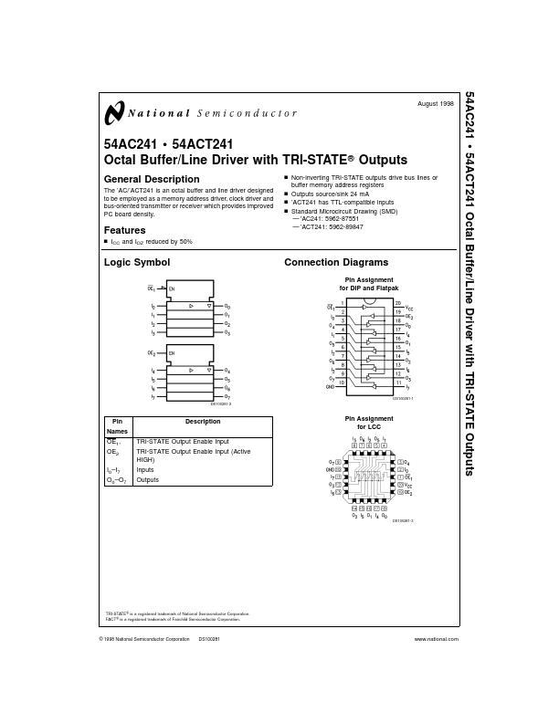
The ’AC/’ACT241 is an octal buffer and line driver designed to be employed as a memory address driver, clock driver and bus-oriented transmitter or receiver which provides improved PC board density. n Non-inverting TRI-STATE outputs drive bus lines or buffer memory address registers n Outputs source/sink 24 m A n ’ACT241 has TTL-patible inputs n Standard Microcircuit Drawing (SMD)
- ’AC241: 5962-87551
- ’ACT241: 5962-89847
Features n ICC and IOZ reduced by 50%
Logic Symbol
Connection Diagrams
Pin Assignment for DIP and Flatpak
DS100281-1 DS100281-2
Pin Names OE1, OE2 I0- I7 O0- O7
Description
TRI-STATE Output Enable Input TRI-STATE Output Enable Input (Active HIGH) Inputs Outputs
Pin Assignment for LCC
DS100281-3
TRI-STATE ® is a registered trademark of National Semiconductor Corporation. FACT ® is a registered trademark of Fairchild Semiconductor Corporation.
© 1998 National Semiconductor Corporation
DS100281
.national.
Truth Tables
Inputs OE1 L L H Inputs OE2 H H L
H = HIGH Voltage Level L = LOW Voltage Level X = Immaterial Z = High Impedance
Outputs In L H X (Pins 12, 14, 16, 18) L H Z Outputs In L H X (Pins 3, 5, 7, 9) L H Z
.national.
Absolute Maximum Ratings (Note 1)
If Military/Aerospace specified devices are required, please contact the National Semiconductor Sales Office/ Distributors for availability and specifications. Supply Voltage (VCC) DC Input Diode Current (IIK) VI =
- 0.5V VI = VCC + 0.5V DC Input Voltage (VI) DC Output Diode Current (IOK) VO =
- 0.5V VO = VCC + 0.5V DC Output Voltage (VO) DC Output Source or Sink Current (IO) DC VCC or Ground Current per Output Pin (ICC or IGND) Storage Temperature (TSTG) Junction Temperature (TJ) CDIP
- 0.5V to +7.0V
- 20 m A +20 m A
- 0.5V to VCC + 0.5V
- 20 m A +20 m A
- 0.5V to VCC + 0.5V
Remended Operating Conditions
Supply Voltage (VCC) ’AC ’ACT Input Voltage (VI) Output Voltage (VO) Operating Temperature (TA) 54AC/ACT Minimum Input Edge Rate (∆V/∆t) ’AC Devices VIN from 30% to 70% of VCC...