GENERAL DESCRIPTION
FEATURES
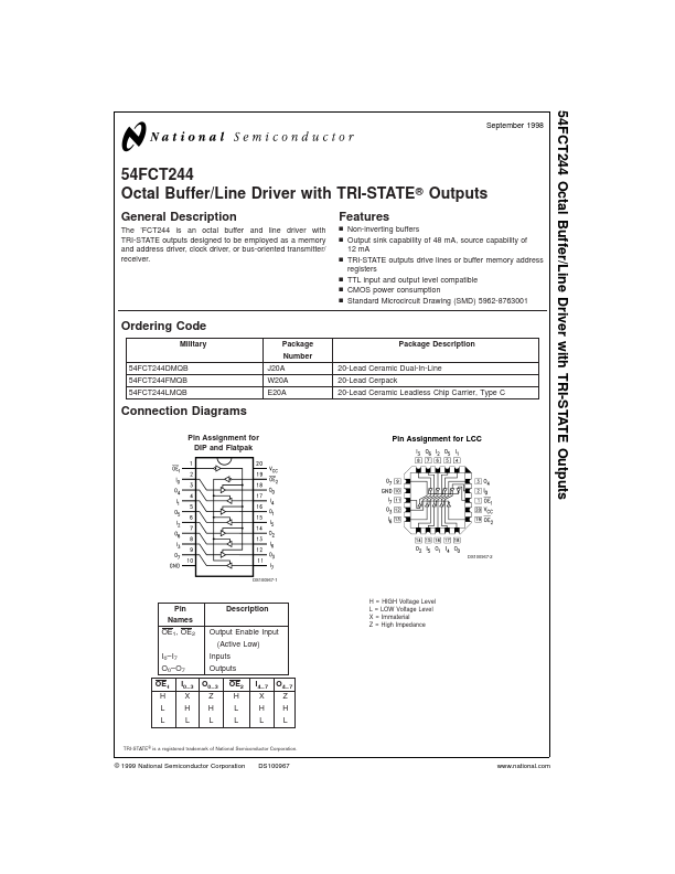
n Non-inverting buffers n Output sink capability of 48 mA, source capability of 12 mA n TRI-STATE outputs drive lines or buffer memory address registers n TTL input and output level compatible n CMOS power consumption n Standard Microcircuit Drawing (SMD) 5962-8763001 Ordering Code Military 54FCT244DMQB 54FCT244FMQB 54FCT244LMQB Connection Diagrams Package Number J20A W20A E20A Package DESCRIPTION
20-Lead Ceramic Dual-In-Line 20-Lead Cerpack 20-Lead Ceramic Leadless Chip Carrier, Type C Pin Assignment for DIP and Flatpak Pin Assignment for LCC DS100967-1 Pin Names OE1, OE2 I0– I7 O0– O7 DESCRIPTION
Output Enable Input (Active Low) Inputs Outputs OE1 H L L I0–3 O0–3 XZ HH LL OE2 H L L I4–7 O4–7 XZ HH LL TRI-STATE® is a registered trademark of National Semiconductor Corporation. © 1999 National Semiconductor Corporation DS100967 DS100967-2 H = HIGH Voltage Level L = LOW Voltage Level X = Immaterial Z = High Impedance 54FCT244 ABSOLUTE MAXIMUM RATINGS
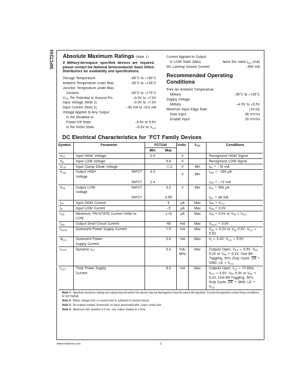
(Note 1)... National Semiconductor