54LS175
Description
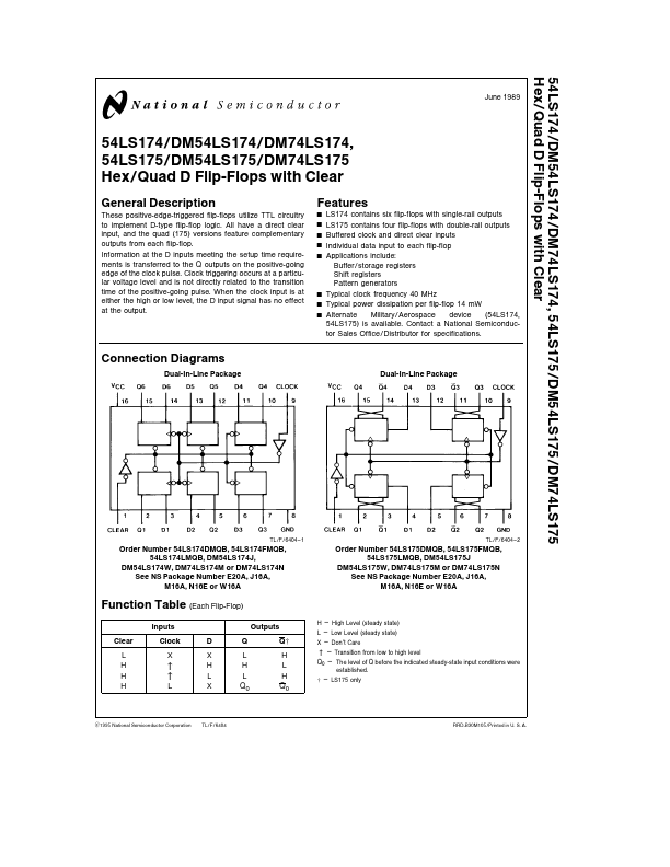
These positive-edge-triggered flip-flops utilize TTL circuitry to implement D-type flip-flop logic All have a direct clear input and the quad (175) versions feature plementary outputs from each flip-flop Information at the D inputs meeting the setup time requirements is transferred to the Q outputs on the positive-going edge of the clock pulse Clock triggering occurs at a particular voltage level and is not directly related to the transition time of the positive-going pulse When the clock input is at either the high or low level the D input signal has no effect at the output.