Description
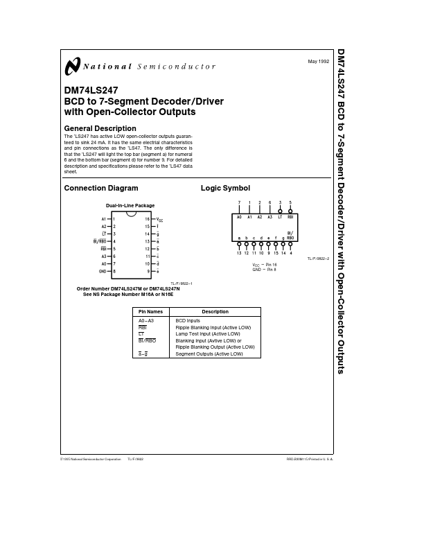
The ’LS247 has active LOW open-collector outputs guaranteed to sink 24 mA It has the same electrial characteristics and Connection Diagram Logic Symbol Dual-In-Line Package May 1992 TL F 9822 – 1 Order Number DM74LS247M or DM74LS247N See NS Package Number M16A or N16E VCC e Pin 16 GND e Pin 8 Pin Names A0 – A3 RBI LT BI RBO a–g Description BCD Inputs Ripple Blanking Input (Active LOW) Lamp Test Input (Active LOW) Blanking Input (Avtive LOW) or Ripple Blanking Output (Active LOW) Segment Outputs (Active LOW) TL F 9822 – 2 C1995 National Semiconductor Corporation TL F 9822 RRD-B30M115 Printed in U S A Supply Voltage 7V Input Voltage 7V Operating Free Air Temperature Range 0 C to a70 C Storage Temperature Range b65 C to a150 C Remended Operating Conditions Symbol VCC VIH VIL IOH IOL TA Parameter Supply Voltage High Level Input Voltage Low Level Input Voltage High Level Output Current BI RBO Low Level Output Current Free Air Operating Temperature Note The ‘‘ Min Nom Max Units 4 75 5 5 25 V 2V 08 V b50 mA 24 mA 0 70 C Symbol Parameter Conditions VI VOH IOFF Input Clamp Voltage High Level Output Voltage Output High Current Segment Outputs VCC e Min II e b 18 mA VCC e Min IOH e Max VIL e Max VCC e 5 5V VO e 15V BI RBO a–g VOL Low Level Output Voltage VCC e Min IOL e Max VIH e Min a – g IOL e 3 2 mA BI RBO IOL e 12 mA a–g IOL e 1 6 mA BI RBO II Input Current Max VCC e Max VI e 7V Input Voltage IIH High Level Input Current VCC e Max VI e 2 7V IIL Low Level Input Current VCC e Max VI e 0 4V Other Inputs VCC e Max VI e 0 4V BI RBO Input IOS Short Circuit Output Current VCC e Max (Note 2) ICC Supply Current VCC e Max Note 1 All typicals are at VCC e 5V TA e 25 C Note 2 Not more than one output should be shorted at a time and the duration should not exceed one second Min 24 b0 3 Typ (Note 1) 34 0 35 0 25 Max b1 5 250 05 05 04 04 01 20 b0 4 b1 2 b2 0 13 Units V V mA V mA mA mA mA mA mA Switching Characteristics VCC e a5V TA e a25 C Symbol Parameter tPLH Propagation Delay Time Low to High Level Output tPHL Propagation Delay Time High to Low Level Output RL e 2 kX CL e 15 pF Min Max 100 100 Units ns ns 2 Physical Dimensions inches (millimeters) 16-Lead Small Outline Molded Package (M) Order Number DM74LS247M NS Package Number M16A 3 DM74LS247 BCD to 7-Segment Decoder Driver with Open-Collector Outputs Physical Dimensions inches (millimeters) (Continued) 16-Lead Molded Dual-In-Line Package (N) Order Number DM74LS247N NS Package Number N16E LIFE SUPPORT POLICY NATIONAL’S PRODUCTS ARE NOT AUTHORIZED FOR USE AS CRITICAL PONENTS IN LIFE SUPPORT DEVICES OR SYSTEMS WITHOUT THE EXPRESS WRITTEN APPROVAL OF THE PRESIDENT OF NATIONAL SEMICONDUCTOR CORPORATION As used herein 1 Life support devices or systems are devices or systems which (a) are intended for surgical implant into the body or (b) support or sustain life and whose failure to perform when properly used in accordance with instructions for use provided in the labeling can be reasonably expected to resul.