74C932
74C932 is MM74C932 manufactured by National Semiconductor.
Description
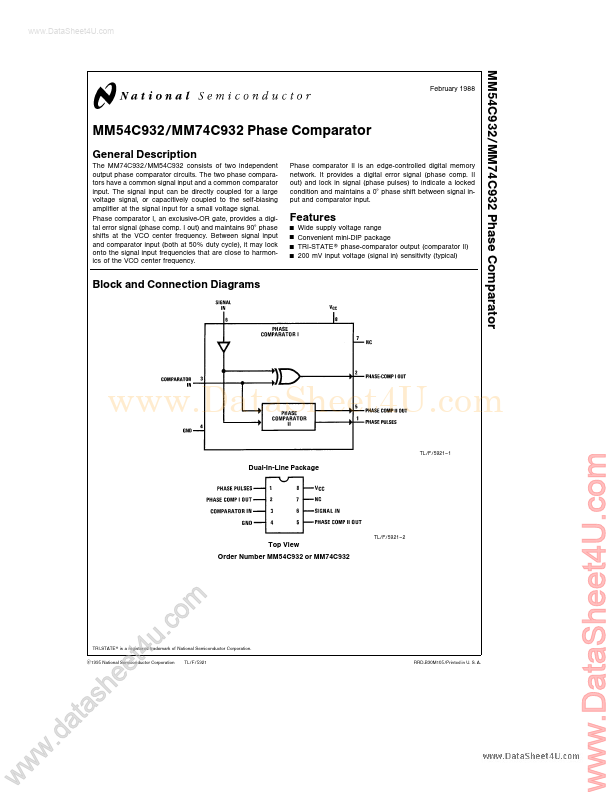
The MM74C932 MM54C932 consists of two independent output phase parator circuits The two phase parators have a mon signal input and a mon parator input The signal input can be directly coupled for a large voltage signal or capacitively coupled to the self-biasing amplifier at the signal input for a small voltage signal Phase parator I an exclusive-OR gate provides a digital error signal (phase p I out) and maintains 90 phase shifts at the VCO center frequency Between signal input and parator input (both at 50% duty cycle) it may lock onto the signal input frequencies that are close to harmonics of the VCO center frequency Phase parator II is an edge-controlled digital memory network It provides a digital error signal (phase p II out) and lock in signal (phase pulses) to indicate a locked condition and maintains a 0 phase shift between signal input and parator input
Features
Wide supply voltage range Convenient mini-DIP package TRI-STATE phase-parator output (parator II) 200 m V input voltage (signal in) sensitivity (typical)
Block and Connection Diagrams
..
TL F 5921- 1
Dual-In-Line Package
TL F 5921- 2
Top View Order Number MM54C932 or MM74C932
TRI-STATE is a registered trademark of National Semiconductor Corporation C1995 National Semiconductor Corporation w w w
.d h s a t a ee
. u t4 m o c
TL F 5921 RRD-B30M105 Printed in U S A
..
..
Absolute Maximum Ratings (Note 1)
If Military Aerospace specified devices are required please contact the National Semiconductor Sales Office Distributors for availability and specifications Voltage at Any Pin Operating Temperature Range MM54C932 MM74C932 Storage Temperature Range b 0 3V to VCC a 0 3V b 55 C to a 125 C b 40 C to a 85 C b 65 C to a 150 C
Power Dissipation (PD) Dual-In-Line Small Outline Operating VCC Range Absolute Maximum VCC Lead Temperature (Soldering 10 seconds)
700 m W 500 m W 3V to 15V 18V 260 C
DC Electrical Characteristics
Symbol ICC Parameter Quiescent Device Current...