74LS14
Overview
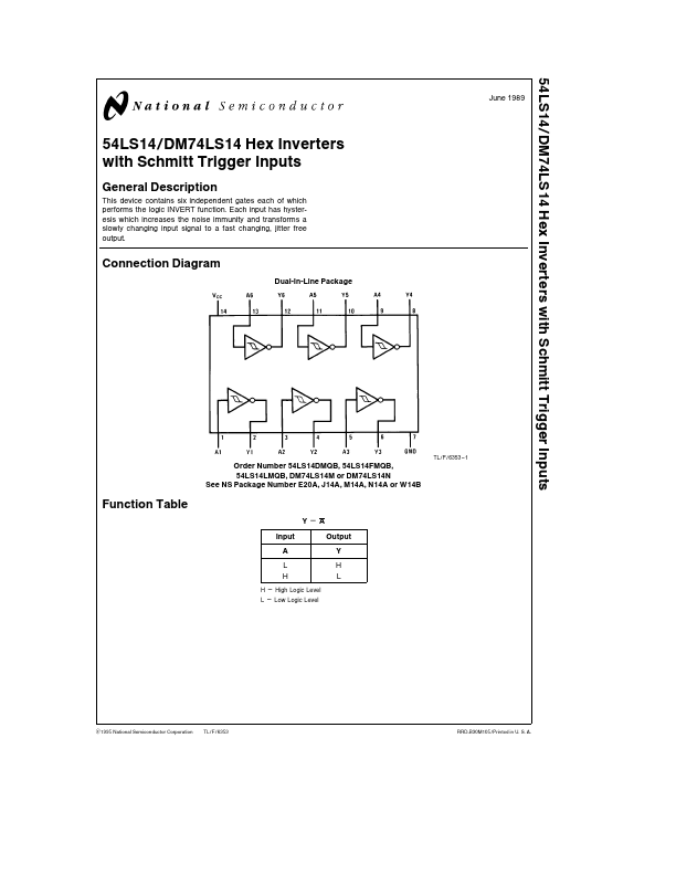
This device contains six independent gates each of which performs the logic INVERT function Each input has hysteresis which increases the noise immunity and transforms a slowly changing input signal to a fast changing jitter free output Connection Diagram Dual-In-Line Package TL F 6353 - 1 Order Number 54LS14DMQB 54LS14FMQB 54LS14LMQB DM74LS14M or DM74LS14N See NS Package Number E20A J14A M14A N14A or W14B Function.