Description
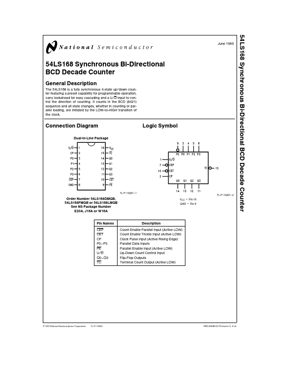
The 54LS168 is a fully synchronous 4-state up down counter featuring a preset capability for programmable operation carry lookahead for easy cascading and a U D input to control the direction of counting It counts in the BCD (8421) sequence and all state changes whether in counting or parallel loading are initiated by the LOW-to-HIGH transition of the clock Connection Diagram Dual-In-Line Package Logic Symbol TL F 10207 - 1 TL F 10207 - 2 Order Number 54LS168DMQB 54LS168FMQB or 54LS168LMQB See NS Package Number E20A J16A or W16A VCC e Pin 16 GND e Pin 8 Pin Names CEP CET CP P0-P3 PE U D Q0-Q3 TC Description Count Enable Parallel Input (Active LOW) Count Enable Trickle Input (Active LOW) Clock Pulse Input (Active Rising Edge) Parallel Data Inputs Parallel Enable Input (Active LOW) Up-Down Count Control Input Flip-Flop Outputs Terminal Count Output (Active LOW) C1995 National Semiconductor Corporation TL F 10207 RRD-B30M105 Printed in U S A (Note) Note The ‘‘ If Military Aerospace specified devices are required please contact the National Semiconductor Sales Office Distributors for availability and specifications Supply Voltage 7V Input Voltage 5 5V Operating Free Air Temperature Range b 55 C to a 125 C 54LS b 65 C to a 150 C Storage Temperature Range Remended Operating Conditions Symbol VCC VIH VIL IOH IOL TA ts (H) ts (L) th (H) th (L) ts (H) ts (L) th (H) th (L) ts (H) ts (L) th (H) th (L) tw (H) tw (L) Parameter Min Supply Voltage High Level Input Voltage Low Level Input Voltage High Level Output Current Low Level Output Current Free Air Operating Temperature Setup Time HIGH or LOW Pn CEP or CET to CP Hold Time HIGH or LOW Pn CEP or CET to CP Setup Time HIGH or LOW PE to CP Hold Time HIGH or LOW PE to CP Setup Time HIGH or LOW U D to CP Hold Time HIGH or LOW U D to CP CP Pulse Width HIGH or LOW b 55 54LS168 Nom 5 Max 55 Units V V 07 b0 4 45 2 V mA mA C ns ns ns ns ns ns ns 4 125 15 15 5 5 20 20 0 0 25 25 0 0 20 20 2 Symbol VI VOH VOL II IIH Parameter Input Clamp Voltage High Level Output Voltage Low Level Output Voltage Input Current Input Voltage Max Conditions VCC e Min II e b18 mA VCC e Min IOH e Max VIL e Max VIH e Min VCC e Min IOL e Max VIH e Min VIL e Max VCC e Max VI e 10 0V VCC e Max VI e 2 7V Inputs CET IIL Low Level Input Current VCC e Max VI e 0 5V Data CP PE U D CEP CET IOS ICC Short Circuit Output Current Supply Current VCC e Max (Note 2) VCC e Max (Note 3) b0 5 b 30 b 60 b 20 Min Typ (Note 1) Max b1 5 Units V V 25 04 01 20 40 b 400 b 400 b 800 b 100 V mA mA High Level Input Current mA mA mA 34 Note 1 All typicals are at VCC e 5V TA e 25 C Note 2 Not more than one output should be shorted at a time and the duration should not exceed one second Note 3 ICC is measured with all outputs open and all inputs grounded Switching Characteristics VCC e a 5 0V TA e a 25 C (See Section 1 for test waveforms and output load) 54LS168 Symbol Parameter Min fMax tPLH tPHL tPLH tPHL tPLH tPHL tPLH tPHL Maximum Clock Frequency Propagation Delay CP to Qn Propagation Delay CP to TC Propagation Delay CET to TC Propagation Delay U D to TC 25 20 20 30 30 15 20 25 25 CL e 15 pF Max MHz ns ns ns ns Units.