ADC08061
Overview
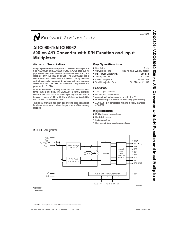
Using a patented multi-step A/D conversion technique, the 8-bit ADC08061 and ADC08062 CMOS ADCs offer 500 ns (typ) conversion time, internal sample-and-hold (S/H), and dissipate only 125 mW of power. The ADC08062 has a two-channel multiplexer.
- n n n
- 1 or 2 input channels No external clock required Analog input voltage range from GND to V+ Overflow output available for cascading (ADC08061) ADC08061 pin-compatible with the industry standard ADC0820