GENERAL DESCRIPTION
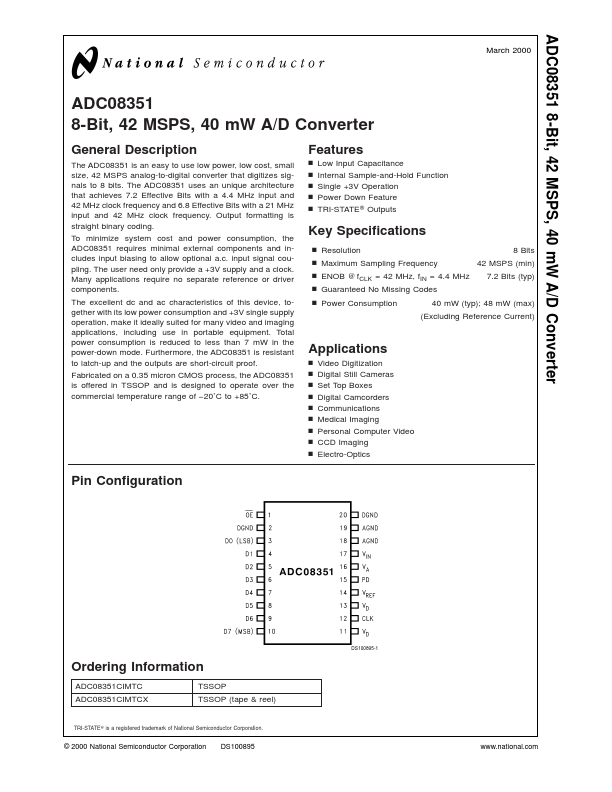
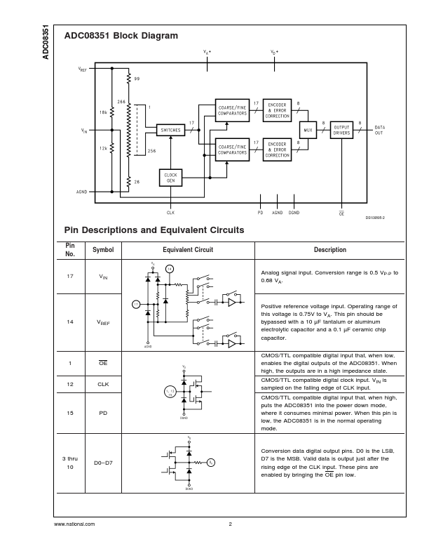
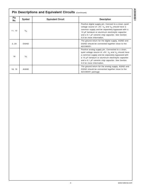
Output formatting is straight binary coding. input signal coupling. The user need only provide a +3V supply and a clock. Many applications require no separate reference or driver components. The excellent dc and ac characteristics of this device, together with its low power consumption and +3V single supply operation, make it ideally suited for many video and imaging applications, including use in portable equipment. Total power consumption is reduced to less than 7 mW in the power-down mode. Furthermore, the ADC08351 is resistant to latch-up and the outputs are short-circuit proof. Fabricated on a 0.35 micron CMOS process, the ADC08351 is offered in TSSOP and is designed to operate over the commercial temperature range of −20˚C to +85˚C. FEATURES
n n n n n Low Input Capacitance Internal Sample-and-Hold Function Single +3V Operation Power Down Feature TRI-STATE ® Outputs Key Specifications n Resolution n Maximum Sampling Frequency n ENOB @ fCLK = 42 MHz, fIN = 4.4 M... National Semiconductor