GENERAL DESCRIPTION
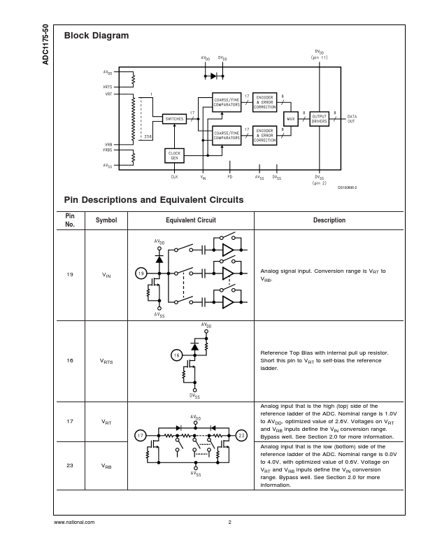
Output formatting is straight binary coding. Furthermore, the ADC1175-50 is resistant to latch-up and the outputs are short-circuit proof. The top and bottom of the ADC1175-50’s reference ladder is available for connections, enabling a wide range of input possibilities. The low input capacitance (7 pF, typical) makes this device easier to drive than conventional flash converters and the power down mode reduces power consumption to less than 5 mW. The ADC1175-50 is offered in SOIC (EIAJ) and TSSOP. It is designed to operate over the commercial temperature range of −20˚C to +75˚C. n Industry standard pinout n Power-down mode ( < 5 mW) Key Specifications n n n n n n n n n Resolution 8 Bits Maximum Sampling Frequency 50 MSPS (min) THD 54 dB (typ) DNL 0.7 LSB (typ) ENOB @ fIN = 25 MHz 6.8 Bits (typ) Guaranteed No Missing Codes Differential Phase 0.5˚ (typ) Differential Gain 1.0% (typ) Power Consumption 125 mW (typ), 190 mW (max) (Excluding Reference Current) APPLICATIONS
... National Semiconductor